Isolating Micro-Machined Die Packaging Stress during Automated Thermal Calibration
Automated thermal calibration must isolate packaging thermo-mechanical stress shifts from intrinsic silicon sensor signals using real-time compensation.
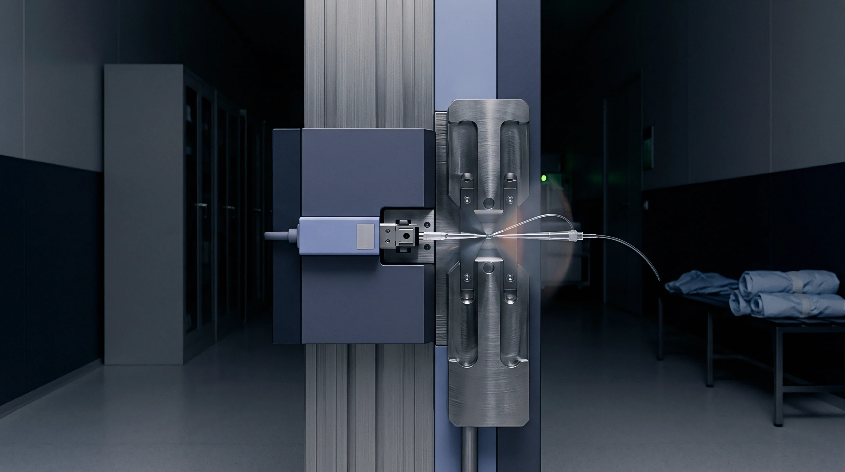

Coupling
Micro-machined silicon elements experience significant compressive loads once encapsulated in organic resin packages. The underlying strain stems from sharp differences in thermal expansion across the package materials. While monocrystalline silicon has a coefficient of thermal expansion near 2.6 parts per million per Kelvin, mold compounds usually sit between 10 and 15 parts per million per Kelvin, and copper alloy leadframes expand at 16.5 parts per million per Kelvin.
As automated handlers sweep devices across calibration temperatures, these mismatched expansion rates generate internal stresses that mechanically distort the micromachined diaphragm or proof mass.
Piezoresistive elements on the die surface convert this packaging strain into resistance changes through piezoresistive coupling. The resulting shear stresses shift the zero-point balance of Wheatstone bridge layouts, producing voltage offsets that calibration hardware registers as applied physical pressure or acceleration. In practice, this thermally induced mechanical offset often exceeds the intrinsic thermal drift of the raw silicon element.
Silicon piezoresistors convert parasitic package shear into zero-point voltage variations that mimic genuine pressure inputs.
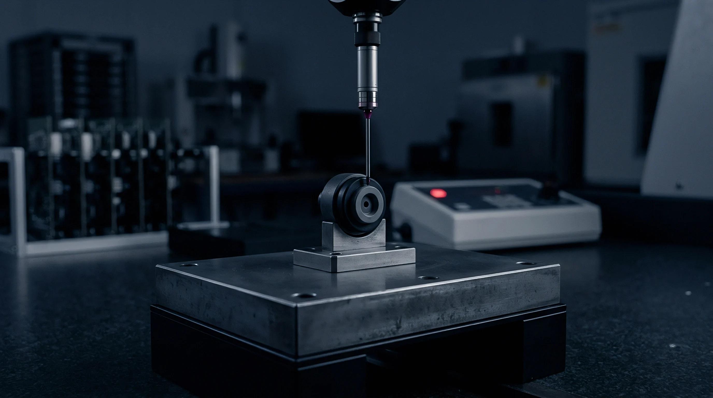
Mechanics of Packaging Strain
In-plane normal stresses and out-of-plane bending moments travel from the encapsulation through the die-attach layer and into the active transducer area. How those stresses distribute depends largely on the glass transition temperature of the epoxy mold compound. Below this point, the polymer matrix stiffens considerably, multiplying the bending force exerted on the silicon die.
Standard calibration routines that assume linear sensor behavior break down when thermal sweeps cross this transition, since the rate of stress change per degree Celsius shifts abruptly.
| Material Phase | Expansion Coefficient (10^-6 / K) | Young’s Modulus (GPa) | Poisson Ratio |
|---|---|---|---|
| Silicon Substrate (100) | 2.6 | 130 | 0.28 |
| Epoxy Mold Compound (Below Tg) | 12.0 | 22 | 0.30 |
| Epoxy Mold Compound (Above Tg) | 45.0 | 2 | 0.45 |
| Copper Alloy Leadframe | 16.5 | 120 | 0.34 |
| Silicone Die Attach Adhesive | 300.0 | 0.003 | 0.49 |
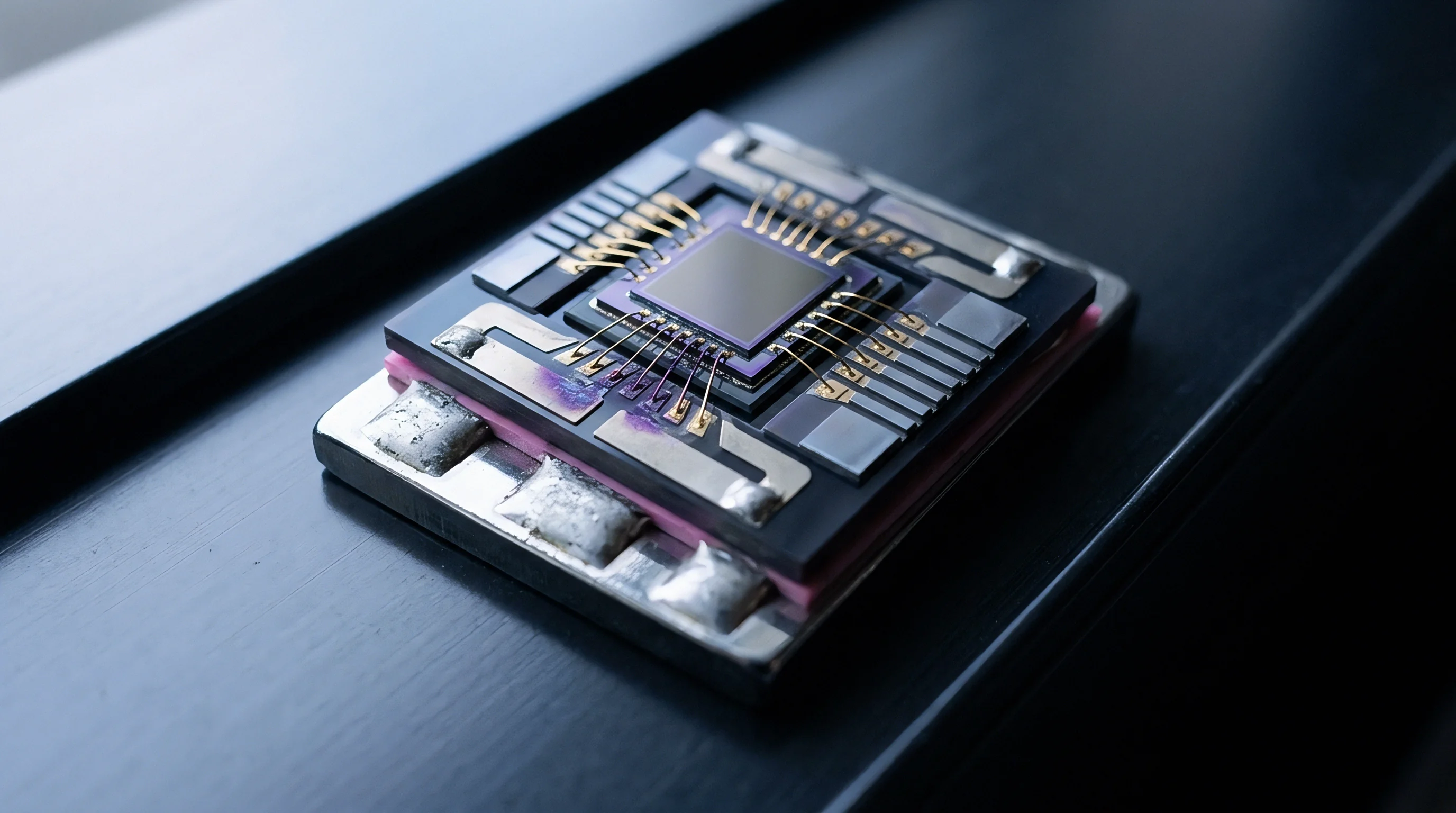
Thermo-Mechanical Coefficient Divergence
Because monocrystalline silicon has anisotropic elastic constants, packaging stresses do not resolve evenly across crystallographic axes. Uniform external pressure creates distinctly asymmetric resistance shifts in resistors laid out along prime crystal directions. Automated thermal calibration hardware must therefore separate genuine physical measurands from the parasitic stress profiles caused by package geometry.
Ignoring packaging stress during calibration bakes packaging creep directly into the calibration matrix, leading to field drift and warranty returns as components relax over time.
Mount
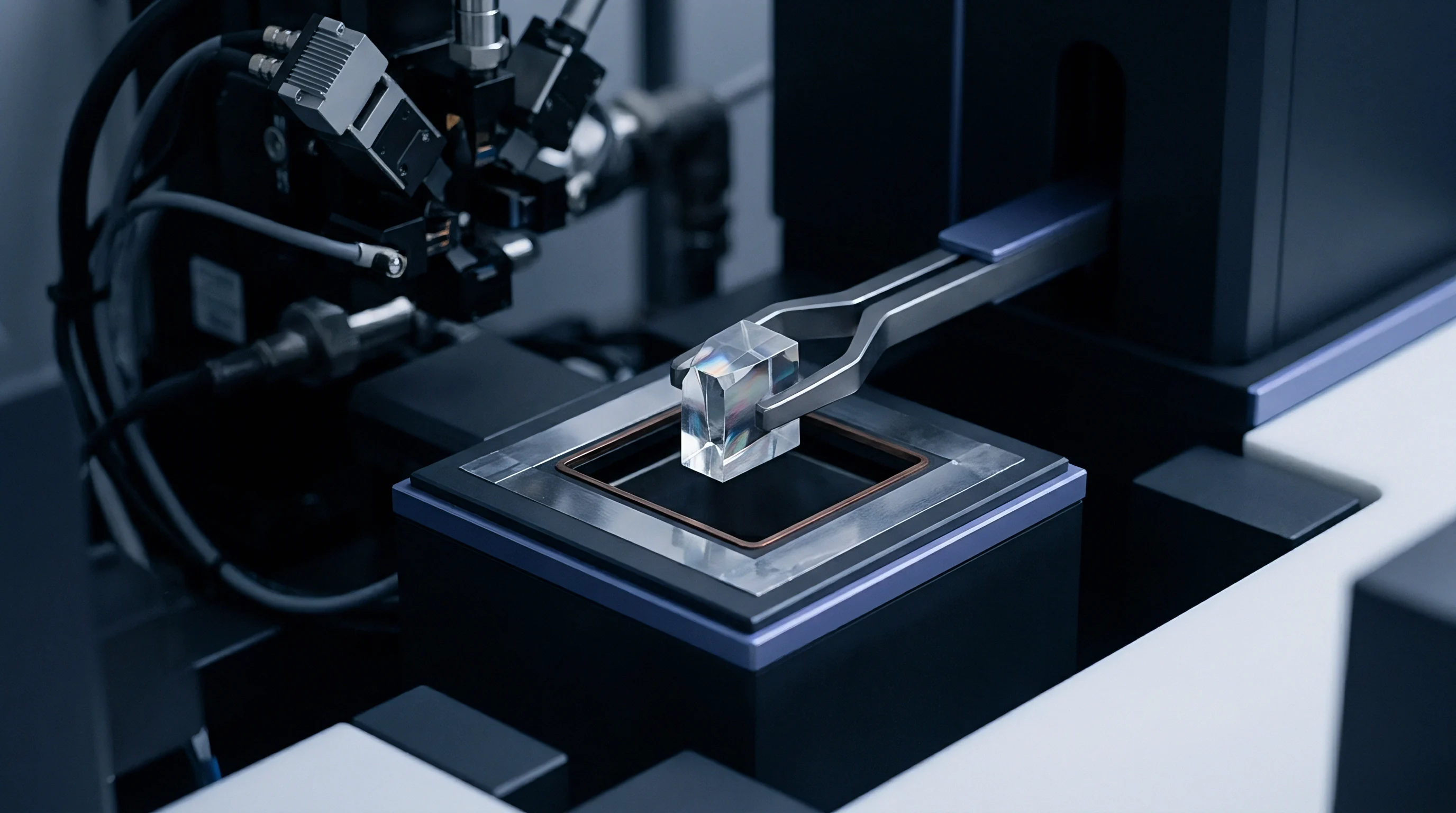
The boundary layer between the silicon chip and its packaging cavity largely governs how much external stress reaches the active transduction zone. Die-attach adhesives serve as the main buffer here. Hard, silver-filled epoxies couple thermal expansion forces directly from the metallic leadframe into the die, whereas compliant silicone adhesives decouple these forces by accommodating shear strain within the bond line.
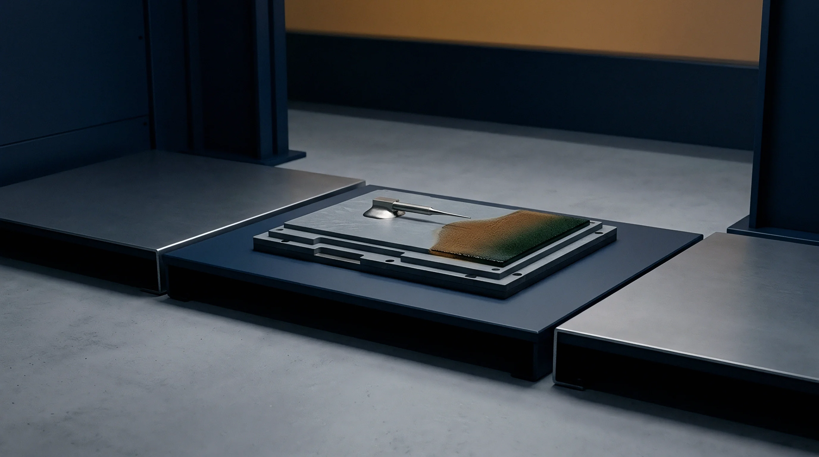
A thicker bond line reduces transmitted shear stress by introducing more mechanical compliance beneath the die. However, thickness variations across a single chip create localized stress gradients, and voiding within the adhesive layer breaks stress symmetry, introducing uncompensated thermal tilt across Wheatstone bridge structures.
Compliant Die Attach Selection
High-speed pneumatic dispensers on automated lines can introduce shot-to-shot volume variations that alter bond line thickness across production lots. Thinner adhesive regions couple more rigidly to the leadframe, widening the spread of thermal offsets observed during high-throughput calibration.
- Socket actuation overload Pin contact forces exceeding two newtons bend the package leadframe during automated handler positioning.
- Asymmetric epoxy bleedout Die-attach adhesive creeping unevenly across chip edges creates localized stress concentrations during thermal expansion.
- Interposer pad warpage Multilayer organic substrates flex unequally along orthogonal axes when exposed to automated thermal shocks.
- Plunger contact friction Mechanical hold-down pins generate lateral shear vectors during rapid temperature transitions in automated test sockets.
AEC-Q103-002 defines acceptable limits for zero-point thermal shift under continuous mechanical clamping during temperature cycling.
Test Socket Strain Injection
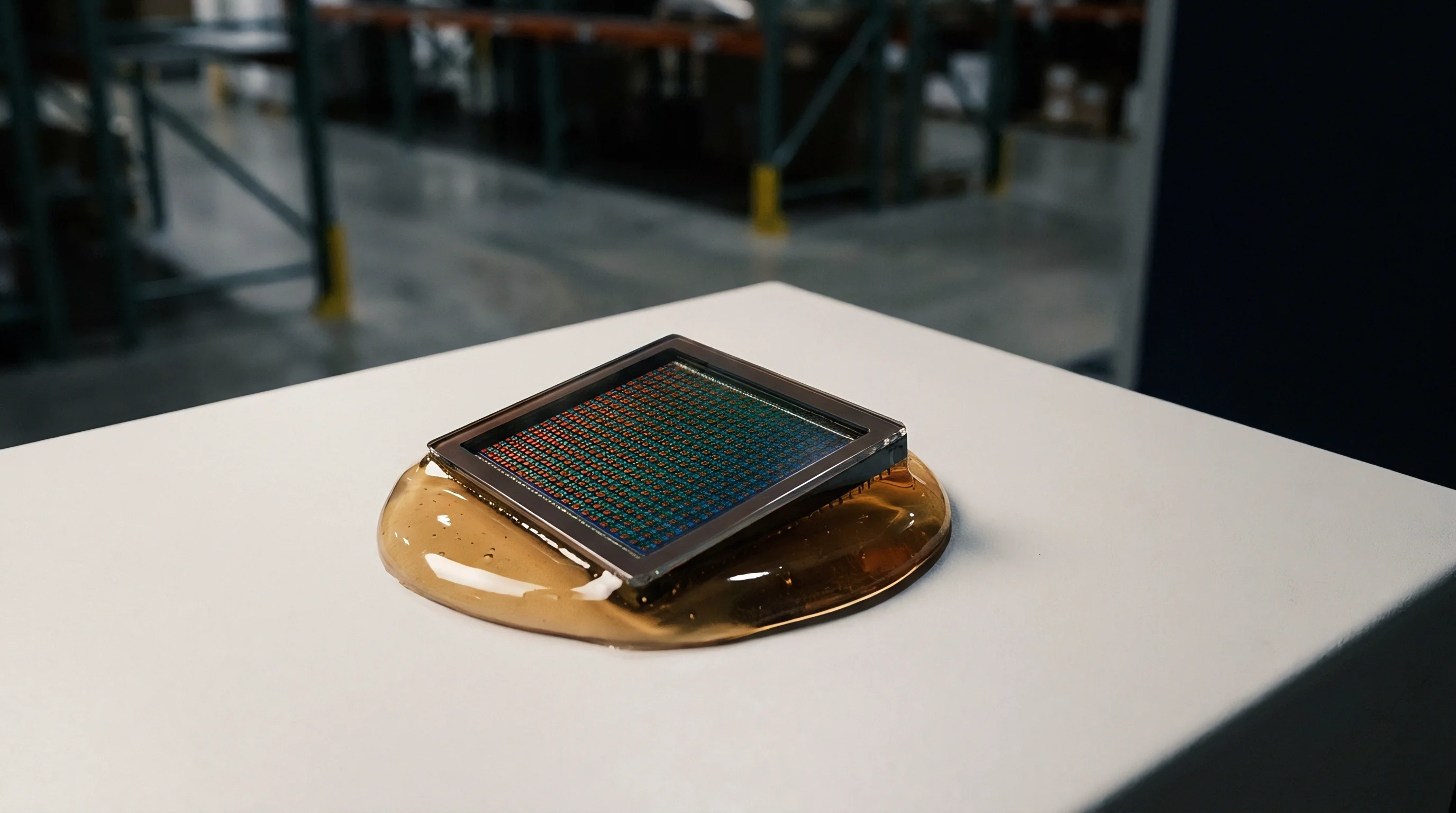
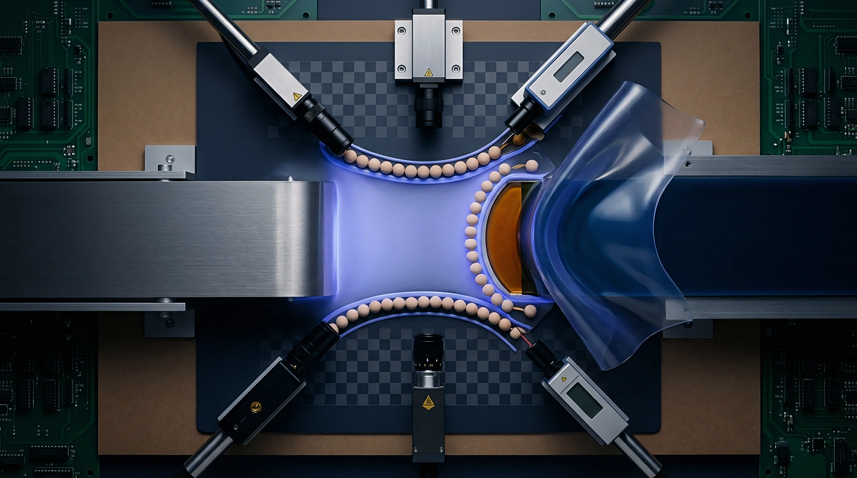
High-speed handlers apply direct mechanical force to hold package terminals against test sockets during thermal sweeps. This clamping load introduces temporary mechanical strain into the package body that superimposes onto thermal packaging stresses, skewing the measurements recorded by test instruments. Calibration terms calculated under socket pressure inevitably drift once the part is released from the test nest.
While soft silicone adhesives absorb packaging stresses effectively, their low shear modulus can allow high-frequency acceleration to shift the die physically within the cavity.
Cycling
Production test cells use aggressive thermal ramps to minimize calibration cycle times. Ramp rates exceeding 10°C per minute set up sharp temperature gradients between the outer plastic packaging and the internal silicon die, with the resin heating or cooling well ahead of the sensor structure.
These transient gradients generate dynamic stress fields that differ substantially from steady-state isothermal conditions. Capturing calibration points before the assembly reaches equilibrium writes systematic offset errors directly into the device’s trim registers.

Can Transient Thermal Gradients Bypass Piezoresistive Offset Trimming?
Transient thermal gradients unbalance piezoresistive bridge symmetry before heat distributes evenly throughout the silicon die. If the automated test system samples output voltages during an active ramp, the acquired data captures non-equilibrium strain states, yielding polynomial fit coefficients that correct for transient thermal gradients rather than true baseline sensor behavior.
Isothermal test routines prevent this by inserting calculated soak times at each calibration temperature node. These dwell periods account for the thermal mass of the contact socket, the package time constant, and the internal thermal resistance of the die attach.
Determining the necessary soak duration requires empirical validation during test cell setup.
- Soak the device at cold soak temperature of -40 degrees Celsius for 120 seconds.
- Record zero-offset output voltage every 500 milliseconds across the dwell window.
- Measure the gradient decay slope until delta output drops below 0.05 percent full scale span per minute.
- Compare transient thermal drift against steady-state baseline readings taken in passive oil bath immersion.
A 10 degree per minute ramp rate induces up to 18 megapascals of transient die stress in epoxy-molded QFN packages before thermal equilibrium settles.
Equilibrium Time Constants in Automated Handlers
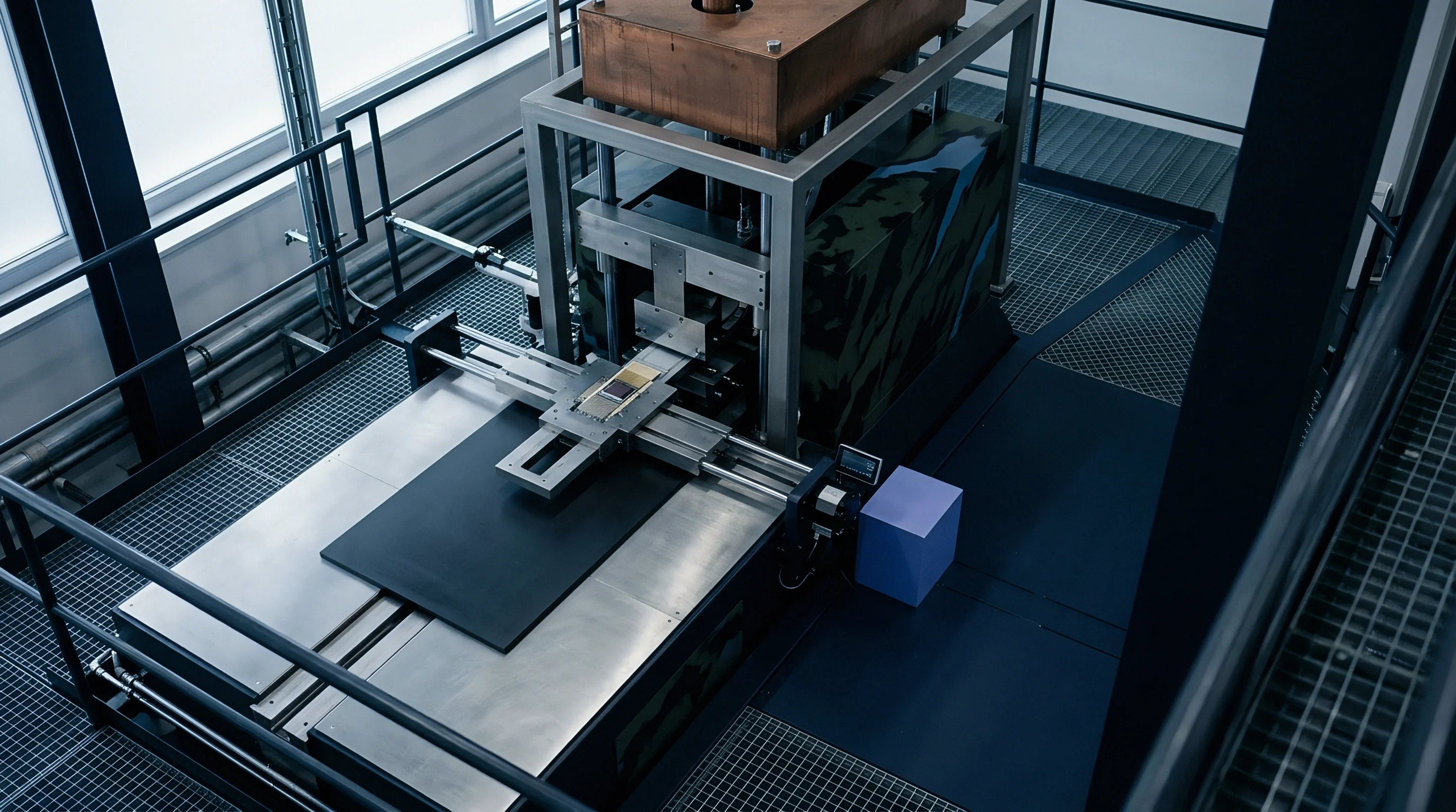
The thermal mass of the test cell governs how quickly the setup reaches isothermal stability. Heavy copper contact blocks increase thermal lag, requiring longer soak windows at each temperature step. Production lines often compress these dwell times to maximize handler throughput, capturing calibration vectors while internal stresses are still settling.
Room-temperature final test data is sometimes treated as sufficient validation, relying on the assumption that packaging stress shifts track nominal polynomial models across temperature.

Correction
Modern sensor architectures counter package strain through real-time mathematical compensation. Dedicated piezoresistive strain bridges are integrated directly onto inactive areas of the die surface, isolated from diaphragm deflection, to isolate and measure package-induced stress independently of the primary sensing structure.
On-chip signal chains digitize both the primary sensor and secondary stress bridge outputs simultaneously. The onboard calibration engine then evaluates multi-variable polynomial equations to cancel out stress-induced offset and sensitivity shifts before outputting data over the digital interface.

On-Die Stress Sensor Extraction
Stress-sensing bridge circuits are oriented specifically to maximize sensitivity to packaging shear while rejecting applied physical measurands. Subtracting the stress bridge signal from the primary sensor output strips out common-mode packaging drift across the full operating range.
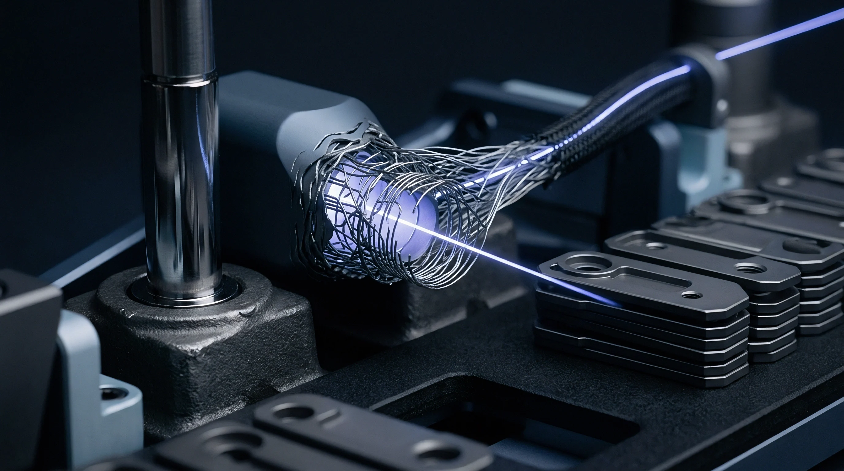
Firmware-driven higher-order polynomial fits compensate for the non-linear thermo-mechanical response around the mold compound’s glass transition. Multi-point thermal calibration cycles generate individual coefficient sets written directly into internal non-volatile memory during automated testing.
| Compensation Architecture | Memory Footprint (Bytes) | Execution Latency (us) | Residual Thermal Shift (% FS) |
|---|---|---|---|
| First-Order Linear Thermal Offset | 64 | 12 | 1.85 |
| Second-Order Temperature Polynomial | 256 | 45 | 0.42 |
| Third-Order Surface Fit with Stress Bridge | 1024 | 135 | 0.05 |
| Lookup Table Interpolation (16 Points) | 2048 | 80 | 0.12 |
Higher-Order Polynomial Fit Calibration
Digital compensation requires precise loading of ASIC memory structures during production testing. The internal signal path processes raw sensor inputs through these correction routines before presenting the data externally.
- Bridge excitation current Precision current sources power on-die stress bridges to prevent self-heating errors from corrupting strain extraction.
- Polynomial coefficient precision Fixed-point thirty-two-bit floating-point registers store strain calibration constants without truncation loss.
- Thermal lookup table granularity Matrix density selections balance non-volatile memory space against residual thermal drift tolerances.
- Non-volatile memory endurance One-time programmable memory blocks seal calibration parameters against unintended field overwrite actions.
On-die piezoresistive stress bridges separate mechanical package loads from environmental temperature changes without increasing calibration cycle times.
ISO 26262 functional safety documentation mandates explicit residual stress error bounds inside the safety element out of context technical specification.


Audit
Production audits monitor the degree to which packaging stress degrades final test yield. Testing wafers prior to assembly establishes intrinsic baseline performance, and comparing those results against post-packaging thermal test data isolates the mechanical offset introduced by the mold compound.
Sourcing strategy balances the lower unit cost of fully molded plastic encapsulation against the superior thermal stability of cavity-seal ceramic packages. Sourcing sensor dies from multiple semiconductor foundries introduces variance in substrate stiffness and piezoresistive coefficient profiles. Packaging lines using alternate mold compound formulas generate distinct thermo-mechanical stress curves that require customized calibration coefficient boundaries inside automated handler software.

Yield Impact of Package Stress Tolerances
Severe packaging stress can push zero-point offsets beyond the input range of onboard ASIC analog front ends, clipping the signal during thermal sweeps. Automated test floors track yield loss at hot and cold extremes to catch lot-to-lot packaging variations. Elevated failure rates at cold test points typically point to an increased mold compound modulus resulting from incomplete resin curing.
Supplier Qualification Metrics for Encapsulated Dies
Qualification dossiers for sensor lines rely on long-term thermal drift data collected during high-temperature operating life tests. These evaluations highlight slow viscoelastic relaxation in the packaging resin. Mechanically unstable packages continuously drift over their service life, undermining the initial calibration programmed during production testing.
Whether grinding wafers below fifty micrometers completely eliminates package-induced thermal drift or merely transfers mechanical vulnerability to solder ball interconnects remains an open question across high-volume sensor foundries.