Common Centroid Transistor Layout Strategies for Low Drift Bandgap Cores
Common centroid transistor layouts for bandgap cores cancel linear thermal and lithographic gradients, reducing post-packaging output drift below 5 ppm per C.


Geometry
Symmetric element placement inside precision voltage references cancels first-order process and thermal gradients across the silicon substrate. In bandgap reference cores, the output voltage depends directly on the ratio of current densities between two bipolar transistor junctions. A standard Brokaw or Kuijk cell relies on an emitter area ratio, typically 1:8 or 1:24, to generate a thermal voltage proportional to absolute temperature.
When thermal gradients sweep across the die from nearby power stages or external package heatsinks, an asymmetric layout introduces a systematic offset error. That offset skews the temperature coefficient away from zero, leaking uncompensated ppm per degree Celsius drift into the final reference output.

Cross Quad Centroid Arrays
Arranging four bipolar transistors in a square matrix neutralizes linear temperature and doping variations. In a 1:8 core configuration, a single unit transistor sits at the center, surrounded by eight identical unit devices, or eight peripheral transistors are grouped with two diagonally opposing pairs forming the reference device. Cross-quad layouts route matched pairs along two perpendicular axes.
By splitting unit devices into sub-units and wiring diagonally opposite components in parallel, the effective center of mass for both networks converges on the exact same physical coordinate.
Lithographic distortions degrade matching if transistor orientations differ across the core. Oxide thickness variations across a two-millimeter die span can shift gate threshold voltages in MOSFET cores or collector current ratios in bipolar cores by up to 0.1 percent. Cross-quad alignment turns this spatial linear oxide gradient into a common-mode shift, preserving the ratio of current densities across the cell.
A core emitter layout utilizing a 3 by 3 cross-quad array holds offset error under 120 microvolts across a 100 degree Celsius operating span when gradient alignment matches the primary thermal axis.
Matching degrades quickly once layout structures encounter non-uniform boundary conditions. Devices on the outer edge of an array run into proximity effects during plasma etching, line-edge roughness variation, and diffusion thermal reflections from surrounding field oxide.

Dummy Transistor Array Placement
Edge structures experience uneven chemical etching during wafer fabrication. Surrounding the active centroid array with a continuous ring of electrically shorted dummy transistors ensures that every active unit transistor sees identical neighboring geometries. These dummy cells match the poly-silicon gate pitch, metal exposure, and diffusion geometries of the core transistors.
| Layout Structure | Area Ratio Implementation | Linear Gradient Rejection | Lithographic Mismatch Risk | Interconnect Parasitic Overhead |
|---|---|---|---|---|
| Cross-Quad Matrix | 1:4 or 1:8 Interleaved | High | Low | Moderate |
| Quad-Swapped Interdigitated | 1:8 Linear Array | Moderate | Low | Low |
| Concentric Ring Matrix | 1:24 Multi-Ring | High | Moderate | High |
| Common Centroid Hexagonal | 1:6 Radial Array | High | High | High |
The choice of common centroid configuration governs both the initial uncalibrated offset and post-assembly thermal stability. Layout choices alter how vulnerable the bandgap core remains to fabrication defects and thermal gradients across the die.
- Process gradient offset shifts the bandgap output voltage when linear oxide variations cross the array asymmetric to device wiring.
- Boundary edge distortion alters transistor beta and saturation current when dummy cell rings are omitted from outer matrix borders.
- Substrate thermal bias introduces thermal voltage mismatch when nearby power switches radiate heat unevenly across transistor branches.
- Etch rate variation modifies active base-emitter junction dimensions across tightly packed transistor fingers during active trench isolation.
Placing dummy transistors around the outer perimeter of a centroid matrix maintains etch uniformity across active base-emitter junctions.


Grid
Interconnect paths determine the parasitic resistance balance across high-precision current mirror branches. Metal trace resistance in series with low-impedance emitter nodes introduces voltage drops that disrupt the logarithmic relationship between current density and delta base-emitter voltage. Even a ten-milliohm mismatch in series emitter routing produces a temperature-dependent offset, corrupting the drift performance established by common centroid placement.

Parasitic Trace Resistance Balancing
Unbalanced trace lengths in base or emitter lines introduce systematic voltage offsets into the delta base-emitter signal. Reaching the central transistor in a 3 by 3 common centroid matrix takes longer runs than reaching adjacent inner devices. To preserve balance, layouts enforce strict topological symmetry and matched trace widths across all interconnect layers.
Running routing trees with matched path lengths, width profiles, and via counts equalizes the IR drops across every individual collector and emitter finger. Laying these runs in thick top-level aluminum or copper metallization lowers total parasitic resistance, minimizing the absolute impact of any residual routing mismatch across the operating temperature envelope.
Symmetric parasitic routing resistance preserves core ratio accuracy only when metal trace widths match across all emitter branches.

Shielding and Metal Coverage Symmetry
Upper-layer metal fills alter thermal dissipation paths directly above sensitive core transistors. Automated chemical-mechanical polishing density rules mandate dummy metal fills across empty silicon regions. Placing asymmetric fill patterns over a common centroid array creates localized mechanical stress and non-uniform heat spreading, making it critical that metal coverage density above all matched core devices remains equal on every metal layer.
- Construct symmetric star routing nodes for all emitter supply connections on the primary metal layer.
- Equalize via counts and via placement geometry across every individual unit transistor collector contact.
- Route base interconnections on a dedicated signal layer surrounded by quiet ground shielding traces.
- Apply dummy metal fill patterns symmetrically across the entire cell footprint using identical pattern blocks.
Asymmetric parasitic trace resistance inside the emitter network increases second-order temperature drift, forcing expensive secondary thermal calibration cycles at wafer sort.

Stress
Mechanical force transferred from epoxy encapsulation into silicon shifts transistor current gain through piezoresistive coupling. When a wafer is diced, mounted on a leadframe, and encased in mold compound, mismatched thermal expansion coefficients generate residual compressive stress ranging from 50 to 200 megapascals. This pressure changes electron and hole mobility, shifting the collector current ratio between matched devices even when they share a common centroid layout.

Piezoresistive Coefficients in Silicon Substrates
Lattice distortion alters carrier mobility unevenly across PNP and NPN emitter structures. On standard (100) silicon wafers, piezoresistive sensitivity peaks along the primary crystal orientation, which coincides with standard chip layout axes. Compressive packaging stress reduces NPN current gain while raising PNP gain.
Common centroid layouts suppress spatial stress gradients, but packaging stress still shifts baseline reference voltages post-reflow.
Board assembly reflow subjects packages to temperatures exceeding 260 degrees Celsius, inducing permanent mold compound shrinkage and leadframe shift. This displacement registers as output voltage hysteresis during post-assembly bench qualification.
Does Plastic Mold Compound Moisture Absorption Induce Bandgap Drift?
Hygroscopic swelling in plastic packaging transfers mechanical compressive force onto die surfaces over operating lifetimes. As mold compound absorbs atmospheric moisture, it expands and shifts the internal stress distribution. Under prolonged high humidity, this expansion can alter die stress by up to 30 megapascals, producing baseline drift in precision reference cores.
Land pattern choices on the printed circuit board also govern how board flex and package expansion couple into the silicon.
| Package Type | Package Stress Range (MPa) | Typical Drift (ppm per degree C) | Moisture Sensitivity Level | Thermal Hysteresis (ppm) |
|---|---|---|---|---|
| WLCSP-4 (Bare Die) | 10 to 30 | 1.5 to 3.0 | MSL 1 | 15 to 30 |
| QFN-16 (3×3 mm) | 60 to 120 | 3.0 to 8.0 | MSL 3 | 50 to 120 |
| SOIC-8 (Standard) | 80 to 160 | 5.0 to 15.0 | MSL 1 | 80 to 200 |
| Ceramic LCC-8 | 5 to 15 | 0.5 to 1.5 | MSL 1 | 5 to 15 |
Engineers evaluate package variants against mechanical stress profiles and environmental exposure constraints to prevent unexpected drift in field applications.
- Crystal orientation alignment aligns core layout axes at 45-degree angles to primary wafer flat directions, diminishing piezoresistive coupling.
- Package corner avoidance positions the active bandgap centroid at the physical geometric center of the die, far from high-stress die corners.
- PCB anchor placement isolates surface-mount reference ICs from mounting screws, board cutouts, and heavy connectors that transmit mechanical flex.
- Underfill material selection applies localized protective coatings over WLCSP bumps to redistribute mechanical solder joint fatigue strain.
Post-assembly reference shifts trace to printed circuit board reflow profiles rather than internal mold compound shrinkage tolerances.
Fuse
Wafer-level trimming compensates for process mismatches prior to packaging. Normal manufacturing variations alter resistor sheet resistance, transistor saturation currents, and base-emitter voltages. To hit initial voltage targets within 0.05 percent, trim networks are built directly into the bandgap core to adjust current ratio legs or output divider strings.

Polysilicon and Metal Link Trimming Mechanics
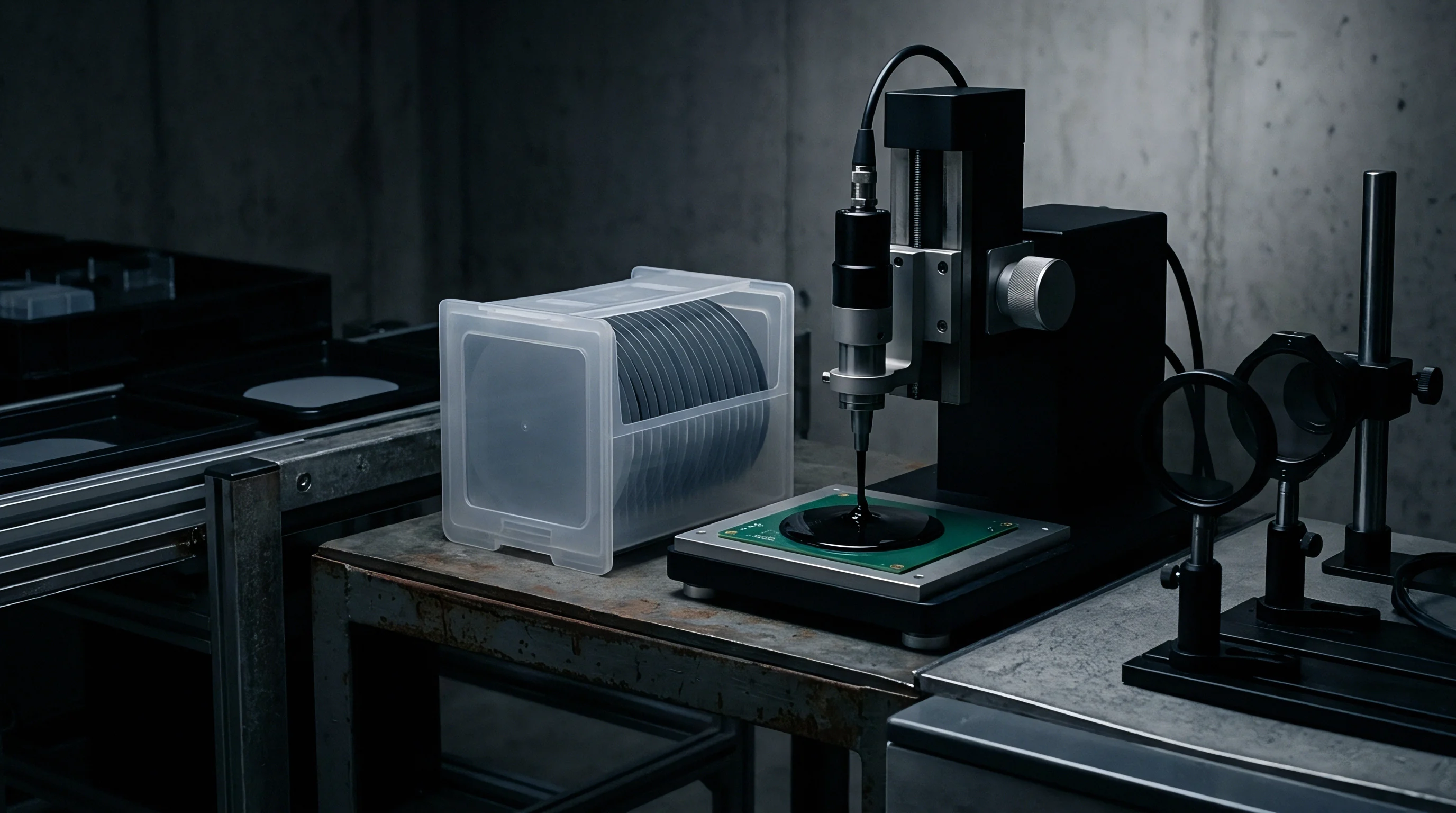
High-current pulses sent through thin resistor segments melt metal connections to reset current mirror ratios. Calibrated bursts from wafer probes sever target polysilicon or aluminum links, altering resistance along the temperature-compensation path in discrete steps. Laser trimming directly ablates thin-film nickel-chromium or tantalum-nitride resistors, providing continuous resistance control without probe contact stress.
Long-term thermal stability depends on link resistance staying constant over time. Blown poly-silicon links can experience regrowth or migration of conductive debris if burn parameters drift outside process margins. Post-trim annealing steps verify insulation integrity across opened links before the die moves to packaging.
Compliance with AEC-Q100 Grade 0 post-reflow drift limits dictates that link burn currents must not exceed oxide thermal breakdown thresholds during wafer sort.
Post Packaging Register Calibration
On-chip non-volatile memory stores calibration values determined after final package reflow. Because plastic packaging introduces stress-induced offsets, trimming at wafer sort cannot correct for assembly-induced shift. OTP digital registers and eFuse structures allow post-packaging trimming over standard serial buses like I2C or SPI.
Digital calibration arrays switch binary-weighted MOSFET gates to steer current into trimming nodes, restoring the target output. Digital trimming avoids physical link oxidation risks while leaving the door open to drift adjustments in the field.
- Laser resistor trimming delivers high precision adjustment on thin-film layers but requires specialized wafer-stage optical alignment equipment.
- Polysilicon link blowing utilizes low-cost wafer probe cards but creates thermal stress spikes near active silicon layers.
- eFuse OTP memory supports post-packaging calibration over standard digital buses, completely eliminating mechanical probe pad requirements.
- Digital interface register override allows live system level offset adjustment during production board bench verification routines.
Section 4.2 of MIL-STD-883 Method 2008 specifies thermal stabilization soak duration prior to trim measurement, preventing false calibration caused by transient junction heating.


Yield
Silicon production economics turn on balancing die area penalties against final package test yields. Implementing common centroid geometries with dummy rings and symmetric routing channels expands bandgap core area by 200 to 400 percent over a basic unmatched topology. In high-volume mixed-signal microcontrollers, that extra analog area lowers net usable die per wafer and drives up baseline silicon cost.

Silicon Area Overhead versus Drift Performance
Adding cells to achieve full common centroid symmetry multiplies the core footprint. A simple 1:8 emitter layout requires nine active unit cells, but adding a full dummy perimeter pushes that count to twenty-five, tripling the silicon consumed by the reference core.
Test duration at wafer sort and final screening directly shapes total landed cost. Multi-temperature sweeps to verify low temperature coefficients add significant runtime on automated test equipment. Deciding between analog common centroid cancellation and digital post-package bus trim creates a direct trade-off between silicon area, test time, and unit pricing.
| Package Variant | Silicon Area Overhead | Wafer Test Time (s) | Trim Resolution (bits) | Minimum Order Quantity | Unit Price at 50k Volume (USD) |
|---|---|---|---|---|---|
| Bare Die (Un-trimmed) | Baseline (1.0x) | 0.2 | None | 10,000 | 0.12 |
| SOIC-8 (Laser Trimmed) | 3.2x Area expansion | 1.8 | 8-bit Analog | 2,500 | 0.45 |
| QFN-16 (eFuse Trimmed) | 2.8x Area expansion | 2.4 | 10-bit OTP | 3,000 | 0.68 |
| WLCSP (OTP Register Trim) | 2.1x Area expansion | 3.1 | 12-bit Digital | 5,000 | 0.82 |
Die area expanded for dummy array termination reduces total usable core wafers per ingot while improving initial untrimmed manufacturing distribution.
Automotive and industrial designs tolerate higher unit costs for common centroid arrays because low intrinsic drift cuts warranty claims and field recalibration expenses. Consumer applications, by contrast, routinely trade thermal stability for lower initial part cost, opting for smaller unmatched cores paired with single-point factory calibration.
Whether advanced multi-point digital calibration in system firmware can economically replace complex multi-layer analog common centroid silicon layouts remains a point of active debate among hardware architects.