Resolving Address Collisions on Multi Sensor Circuit Boards
Resolve multi-sensor address collisions using pin-strapped dividers, digital multiplexers, or active translators sized against bus capacitance and firmware costs.
Strap
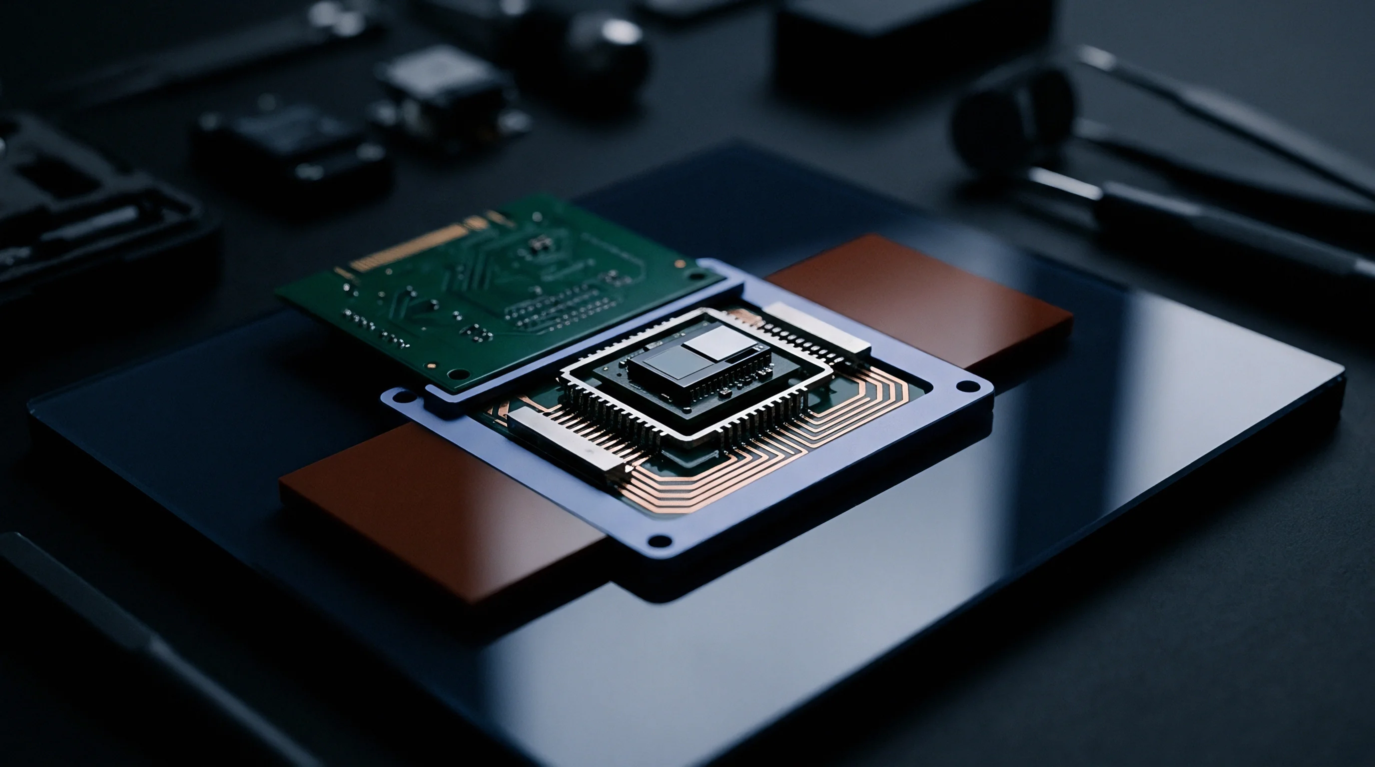
Pin allocation on packaged sensors sets bus architecture long before a board reaches fabrication. Digital environmental sensors, six-axis inertial measurement units, and precision digital temperature monitors frequently offer only one or two hardware address pins. A sensor with an AD0 pin tied to ground or power provides exactly two selectable 7-bit addresses.
Putting four identical sensors on a single printed circuit board creates immediate bus contention unless physical pin strapping distinguishes each device.
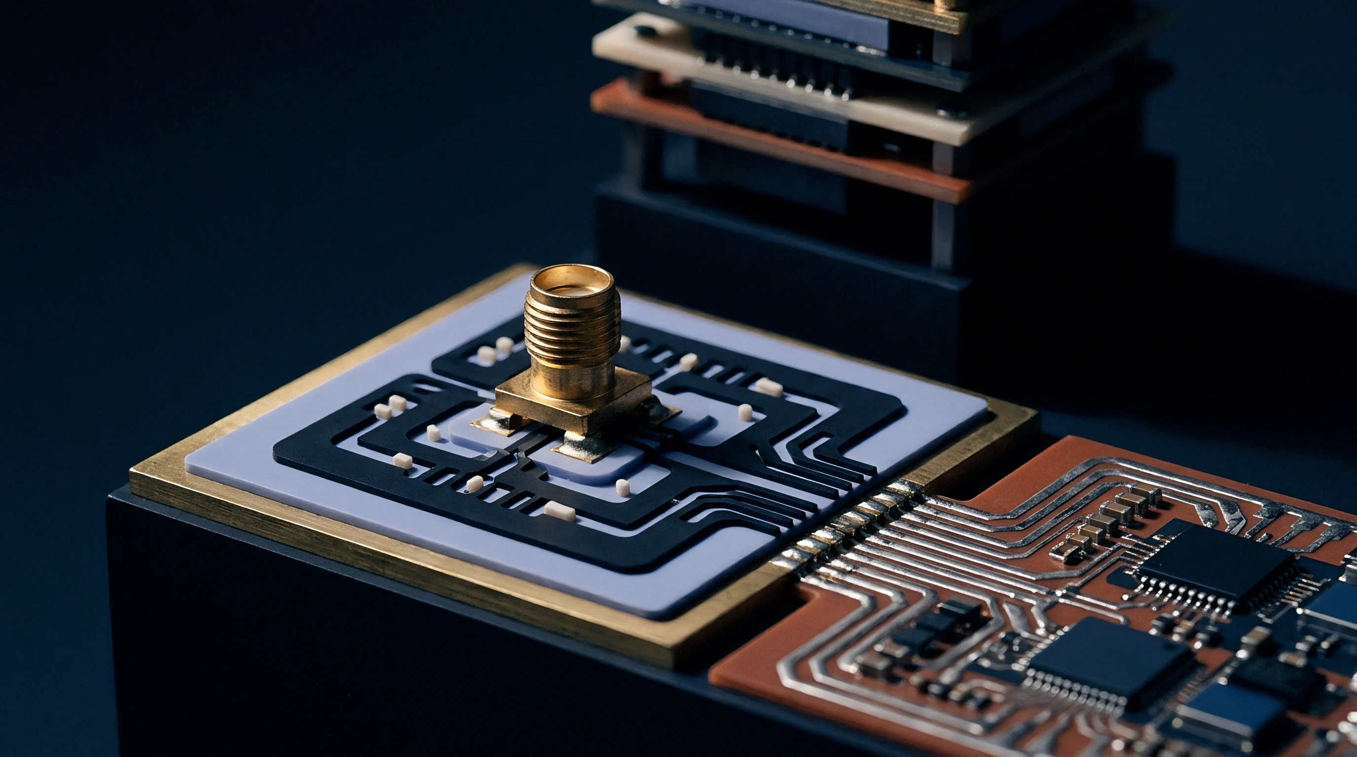
Hardware designers work around this limit by setting electrical potential across discrete pin contacts. Tying address lines to supply rails or ground networks sets fixed binary offsets on the bus interface. Some modern IC packages expand this range by sensing high-impedance states or reading resistive dividers on a single pin during the power-on reset cycle.
Holding an address pin floating, pulled high, pulled low, or terminated with a specific resistor value lets a single die take four discrete slots on the same communication pair.
A pull-down resistor tied to ground establishes the primary base address without adding quiescent current to the battery rail.
Pin-strapped address selection runs into strict electrical limits. Internal pull-up leakage currents, pin capacitance, and noise margins constrain multi-level state detection during startup transients. Internal state machines sample pin voltage within microseconds of supply stabilization.
If trace capacitance slows voltage rise times on an address pin tied to an RC network, the die latches an incorrect bit configuration, permanently shifting its bus address until the next power cycle.

Voltage Divider Sizing for Single Pin Encoding
Selecting components for three-state or four-state pin detection requires tight resistor tolerances. Data sheets typically specify 1% metal film resistors to prevent threshold overlap across temperature extremes. Thermal drift across industrial operating bands from negative 40 degrees Celsius to positive 85 degrees Celsius shifts midpoint voltages toward neighboring comparator windows.
Circuit designers protect noise margins by keeping trace lengths under twenty-five millimeters between the sensing terminal and adjacent bypass components.
| Sensor Type | Package Style | Dedicated Pins | Strapping States | Available Addresses | Nominal 7-Bit Hex Range |
|---|---|---|---|---|---|
| Triple-Axis Accelerometer | LGA-12 (2×2 mm) | 1 (SA0) | 2 (GND, VDD) | 2 | 0x18, 0x19 |
| Temperature and Humidity | DFN-8 (2×2 mm) | 1 (ADDR) | 2 (GND, VDD) | 2 | 0x44, 0x45 |
| Barometric Pressure | LGA-8 (2×2.5 mm) | 1 (SDO) | 2 (GND, VDDIO) | 2 | 0x76, 0x77 |
| Six-Axis Inertial Module | LGA-14 (2.5×3 mm) | 1 (SA0) | 2 (GND, VDDIO) | 2 | 0x68, 0x69 |
| Digital Optical Monitor | DFN-6 (2×2 mm) | 1 (ADR) | 4 (GND, VDD, SDA, SCL) | 4 | 0x29, 0x39, 0x44, 0x45 |
The table highlights a common procurement limit: two addresses are the hard ceiling for standard packaged parts. An architecture that requires eight identical temperature zones across an industrial cold plate runs out of passive configuration options right away. Layout teams are then stuck with routing bloat if they run individual address-select traces to separate host GPIOs.
Directly controlling address lines via GPIO allows dynamic re-addressing at runtime. The host firmware holds three sensors at address 0x44 while pulling the fourth pin high to 0x45 to complete a transfer. This approach introduces strict timing constraints.
Sensor state machines can require up to fifty microseconds to settle after a pin state changes, and polling errors occur if communication starts before the internal Schmitt trigger registers the logic shift.
Dedicated address pins increase package footprint and solder joint counts. To cut mechanical size, package designers eliminate auxiliary control pads on low-profile wafer-level chip scale packages, leaving the silicon locked to a single factory-trimmed address. Passive pin strapping is useless when the device has no external selector pin at all.
Keep address trace stubs short to prevent false latching during a cold system boot.
Switch
Isolating bus segments physically solves address collisions by placing identical silicon dies behind controlled bidirectional gates. An upstream digital controller manages multiple downstream sub-buses through multiplexer ICs like eight-channel pass-gate switches. Upstream traffic passes only to the active downstream segment, leaving all isolated channels disconnected and idle.
Pass-element devices add series channel resistance directly into clock and data lines. An on-resistance between four and twenty-five ohms alters bus fall times and degrades low-level output voltage margins. Downstream pull-up resistors form a voltage divider with the pass-gate resistance during low-side drive phases, which can keep the bus line from reaching standard negative noise margins and cause intermittent ACK failures.
A total capacitive load exceeding four hundred picofarads degrades signal edges beyond specification boundaries under standard bus operating speeds.
Decoupling bus capacitance is the main electrical benefit of segmenting switches. The upstream controller sees only the physical capacitance of the active segment plus the multiplexer’s internal parasitic capacitance. Spreading multiplexers across dispersed sensor arrays keeps bus capacitance below the standard four-hundred-picofarad limit, allowing dense layouts without dropping clock speeds from Fast-mode four hundred kilohertz down to standard hundred kilohertz baselines.

Could Dynamic Channel Selection Induce Deadlocks?
Downstream communication failures lock up the system bus if a target device freezes mid-byte while holding the serial data line low. The host master cannot send a stop condition while the physical data line is pinned near ground. If this lockup happens on an active multiplexer channel, the fault propagates upstream, shutting down communication across every peripheral channel.
Recovering from this requires hardware support. Using a multiplexer without a hardware reset pin introduces substantial risk in field deployments. When a slave holds the line low, the host microcontroller toggles the multiplexer reset line to isolate the faulty branch immediately, then issues nine clock pulses on the cleared segment to reset the stuck slave shift register back to idle.
Downstream switching trees add software overhead. Every transaction directed at a sensor needs a preceding write command to set the multiplexer to the right output path. Bus bandwidth drops as message frequency rises; polling six identical pressure sensors at high rates wastes significant clock cycles just configuring register pointers in the switch.
Latent state errors occur when interrupt lines bypass the multiplexer structure. Routing interrupts through a central switch masks where an alert originated until firmware polls each downstream segment in sequence. Running discrete interrupt traces directly from each sensor to host microcontroller GPIOs removes these delays, though the additional traces take up space on outer board layers and consume microcontroller input pins.
Package choice affects surface-mount assembly yield. Compact twenty-four-lead QFN and TSSOP packages have tight solder paste tolerances on dense boards. Solder bridges between adjacent bus lines under leadless or small-pitch packages force the use of automated optical inspection and post-reflow X-ray testing.
A misaligned pass-gate IC can corrupt multiple downstream channels and block testing during board bring-up.
Improper multiplexer isolation leaves unaddressed downstream branches floating into undefined logic levels.

Bridge
Inline address translation modifies bytes directly on communication wires without requiring software multiplexer commands. Active translator ICs intercept the 7-bit peripheral address byte sent by the master in real time. Hardwired input voltages or external resistor dividers on the translator establish an offset value, and the IC recalculates the address bits on the fly before passing the frame to the peripheral, leaving all subsequent register data untouched.
Translator ICs modify address frames mathematically, typically using a bitwise XOR between the incoming address and an offset vector. A sensor hardwired to address 0x68 can appear externally as 0x69, 0x6A, or 0x6B depending on resistor strapping on the bridge pins. Downstream hardware operates unaware of the remapped address seen by host firmware.
Resistor Configuration Networks for Address Offsets
Active translators use precision resistor dividers to set target address offsets. Dual-pin input networks sample analog voltages using internal analog-to-digital converters during startup. Board layout rules require tight component placement here to keep electromagnetic noise from switching power supplies from corrupting the analog offset levels.
| Divider Voltage Ratio (V_IN / V_DD) | Resistor R1 (kOhm, 1%) | Resistor R2 (kOhm, 1%) | XOR Address Offset (Hex) | Input Address | Translated Bus Address |
|---|---|---|---|---|---|
| 0.000 to 0.095 | Open | 0 (Short) | 0x00 | 0x68 | 0x68 |
| 0.105 to 0.190 | 976 | 147 | 0x01 | 0x68 | 0x69 |
| 0.205 to 0.290 | 845 | 255 | 0x02 | 0x68 | 0x6A |
| 0.305 to 0.390 | 768 | 383 | 0x04 | 0x68 | 0x6C |
| 0.405 to 0.490 | 698 | 536 | 0x08 | 0x68 | 0x70 |
| 0.505 to 0.590 | 604 | 715 | 0x10 | 0x68 | 0x78 |
Propagation delay is a key factor when adding translation ICs. Bidirectional translators add between thirty and eighty nanoseconds of rise and fall delay to signal paths. When combined with isolators or level shifters, accumulated delays erode bus timing margins, and at four-hundred-kilohertz operation, excess delay can violate standard setup and hold timing windows.
Address mapping plans must be checked against reserved address blocks to prevent unexpected bus conflicts. Reserved ranges include seven-bit addresses like 0x00 for general call commands, 0x01 for start bytes, and 0x78 through 0x7B for high-speed master setup. An offset that accidentally moves an accelerometer address into the 0x78 slot will disable high-speed operations across the whole bus.
Active translation keeps software simple. Device drivers read and write to distinct, fixed addresses without managing multiplexer channels or queuing bus arbitration. Firmware can run standard direct-memory access transactions across multiple sensors simultaneously, reducing thread contention by eliminating the mutual-exclusion locks needed for upstream switches.
IPC-A-610 standards govern acceptable lead-to-pad alignment criteria for tiny ten-lead leadless plastic packages.
Board space requirements change when using dedicated translators. Each translator IC needs its own decoupling capacitor, two pull-up resistors, and two divider resistors. A group of four identical sensors requires three translator chips, taking up to forty square millimeters of board space.
Dense designs must balance this footprint penalty against the routing complexity of running multiple separate buses across inner board layers.
Supply stability for dedicated translation silicon varies. Only a few semiconductor manufacturers produce specialized address translation chips. Relying on a single source exposes production to allocation limits, long lead times, and sudden end-of-life notices, whereas standard multiplexers or GPIO-driven setups offer broader second-source options.
Pin-strapping yields zero field returns compared to dynamic translation architectures.

Split
Separating dense sensor arrays across distinct physical interfaces avoids address contention at the schematic level. Modern microcontrollers feature multiple hardware peripheral controllers with independent serial clock and data lines. Routing separate physical traces places identical sensors onto isolated communication domains, eliminating shared-bus arbitration entirely.
Adding secondary buses consumes valuable microcontroller pins. Four isolated sensor buses require eight dedicated pins, quickly using up available I/O on compact sixty-four-pin packages. When hardware peripherals run out, developers often turn to bit-banging on general digital pins.
This resolves address conflicts but shifts timing burdens directly onto the processor core.
Are Dedicated Host Peripherals Justified?
Timing jitter on bit-banged lines causes decoding errors when high-priority interrupts occur. If the processor services an urgent motor control task while toggling a software clock pin, edge timings can stretch beyond bus specifications. Hardware peripheral controllers avoid this by using autonomous direct memory access engines to perform multi-sensor register reads without processor intervention.
Splitting buses significantly improves bandwidth. Distributing eight identical sensors across two hardware buses doubles effective throughput because the master services four sensors per line simultaneously. Polling loops finish in half the time required by a single-bus multiplexer topology at the same clock frequency.
Design teams implement structured trace routing rules when handling multiple active sensor lines:
- Interconnect trace length remains matched within five millimeters across paired clock and data conduits to eliminate phase skew.
- Adjacent signal spacing maintains a three-to-one distance ratio against neighboring switching nets to suppress cross-talk coupling.
- Return path ground structures run unbroken directly below serial traces on layer two to minimize loop inductance.
- Decoupling capacitors sit within two millimeters of device power pins, preventing transient rail sag during output buffer state switching.
Switching bus architectures altogether removes address limits. Sensors often include four-wire serial peripheral interfaces alongside standard two-wire interfaces. SPI uses dedicated chip-select lines to isolate devices; four identical gyroscopes can share common clock, master-in, and master-out conductors while individual chip-select traces target one sensor at a time.
Moving from two-wire to four-wire buses increases routing density. Each added sensor needs an independent line running from the host controller to the device. On a twelve-sensor board, four-wire routing adds twelve separate chip-select traces across inner layers.
Designers have to weigh this layout footprint against the software simplicity of hardware chip-select control.
Digital isolators and level shifters add complexity when splitting buses across high-voltage domains. Isolated channels require dedicated multi-channel capacitive or optical isolators per line. A multi-bus architecture multiplies galvanic isolator counts by the number of independent domains, increasing bill-of-materials costs and power consumption on industrial telemetry nodes.
Deciding whether processing margins justify the added routing complexity of multiple controllers often stays open until software profiling under worst-case communication loads is complete.
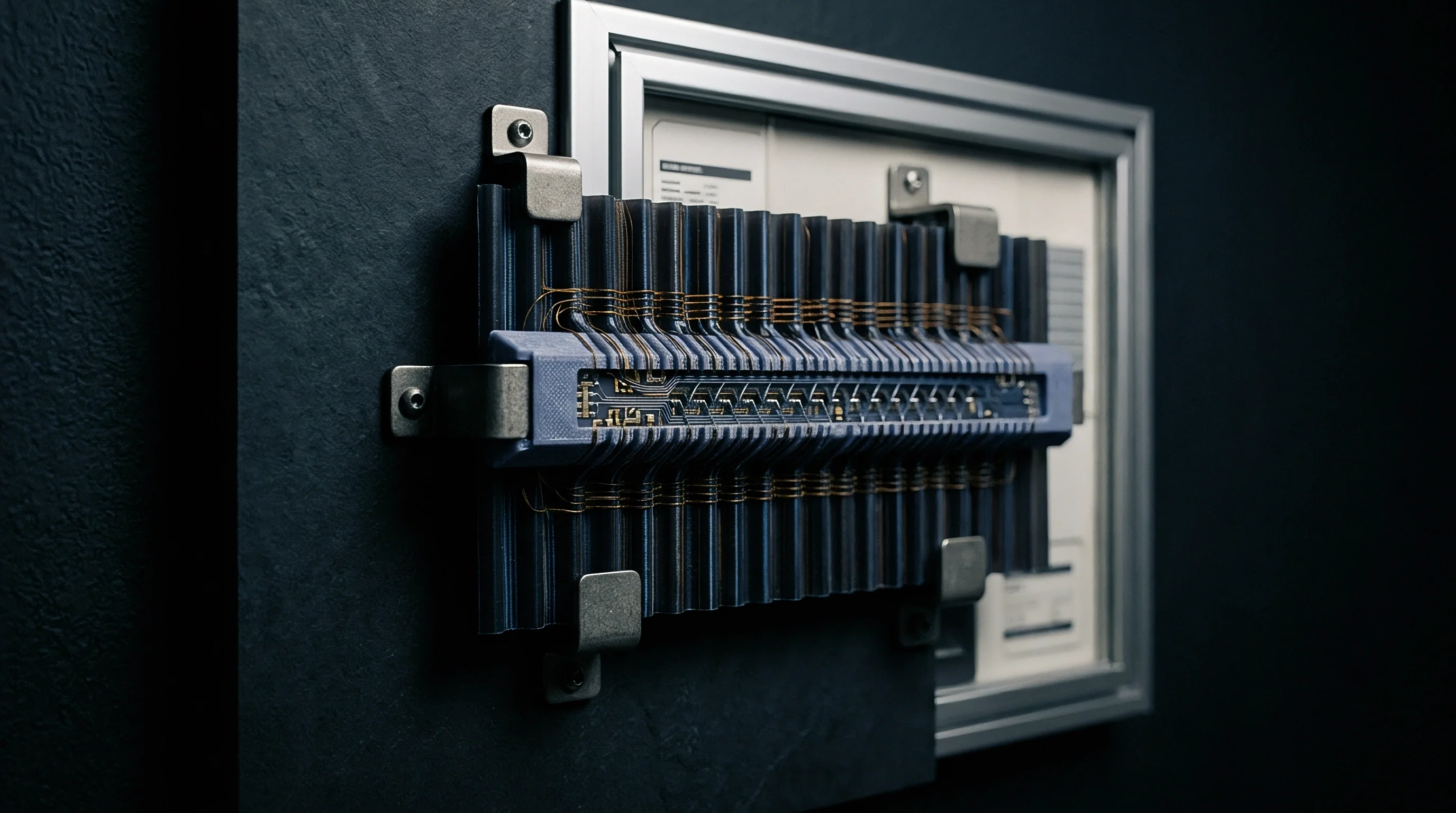
Tariff
Bill-of-materials cost dictates the commercial viability of any multi-sensor address strategy. Sourcing teams compare piece-part prices alongside assembly placement fees, surface-mount yields, and software development effort. A two-cent resistor network for pin strapping easily beats a seventy-cent address translator on cost, assuming the silicon package exposes external address pins.
Assembly costs grow with every discrete component added to the board. Surface-mount placement services bill per component placement. Adding extra pull-up resistors, decoupling capacitors, and translator ICs across eight sensor channels increases unit cost, while additional solder joints raise defect-per-million rates during automated functional testing.
Package selection heavily influences delivered sensor unit pricing. Sensor manufacturers supply identical silicon die layouts across diverse package variants:
- Wafer-level chip scale packages minimize package real estate while restricting address configuration to a single pre-programmed binary identifier. Solder joint failure risks escalate under mechanical board flexure conditions.
- Land grid arrays balance compact footprint boundaries with dual-state pin strapping options, delivering industrial thermal cycling endurance. Reflow profiling mandates precise nitrogen atmosphere controls to prevent void formation.
- Plastic quad flat packages maximize pin counts to expose multi-state address strapping networks, reducing system-level silicon component counts. Unit component pricing rises by twenty to forty percent over bare silicon alternatives.
- Pre-calibrated integrated modules house the sensor die, translation logic, and passive decoupling on a subsidiary circuit board. Delivered component expenses increase tenfold, but assembly risk and firmware development drop significantly.
Firmware development time is a major hidden cost when choosing an architecture. Managing multiplexers in software requires extensive state-machine testing to prevent timing locks and deadlocks. A dedicated hardware bridge or multi-bus architecture simplifies driver code and can cut firmware qualification by several weeks.
In low-volume industrial manufacturing, saving three weeks of engineering time easily outweighs small hardware cost increases over a product’s lifecycle.
| Mitigation Route | Added Component Unit Cost (USD) | Added PCB Surface Area | Firmware Complexity Impact | Failure Rate Risk (DPPM) | Design Scalability Boundary |
|---|---|---|---|---|---|
| Hardware Pin Strapping | 0.01 – 0.04 | Minimal (<5 mm²) | Zero overhead | Low (<10) | 2 to 4 nodes maximum |
| Analog Crosspoint Switch | 0.15 – 0.35 | Moderate (12 – 20 mm²) | Low driver overhead | Moderate (20 – 50) | 4 to 8 nodes per IC |
| Digital Bus Multiplexer | 0.30 – 0.85 | Moderate (15 – 25 mm²) | High state machine overhead | Moderate (30 – 60) | 8 downstream channels |
| Active Address Translator | 0.70 – 1.60 | High (25 – 45 mm²) | Zero overhead | Low (<15) | Up to 127 translated nodes |
| Independent Host Controllers | 0.00 – 0.50 | High (Trace routing tax) | Moderate resource binding | Low (<10) | Limited by MCU I/O pins |
Procurement teams must also evaluate lead-time stability across these approaches. Commodity eight-channel digital multiplexers have multiple pin-compatible sources worldwide. Active translation ICs come from specialized suppliers, where lead times can stretch beyond forty weeks during supply shortages.
Using sole-sourced address translators creates supply-chain risk unless backed by guaranteed inventory reserves.
Break-even math defines when to switch approaches. For production runs under ten thousand units, active translators or integrated sub-modules yield the lowest total cost by minimizing driver development time. Above one hundred thousand units a year, recurring hardware component costs dominate, making pin-strapped packages or direct host routing necessary to strip secondary ICs from the bill of materials.
Standard supply agreements require full re-qualification whenever component substitutions change address pin availability on active production bills.