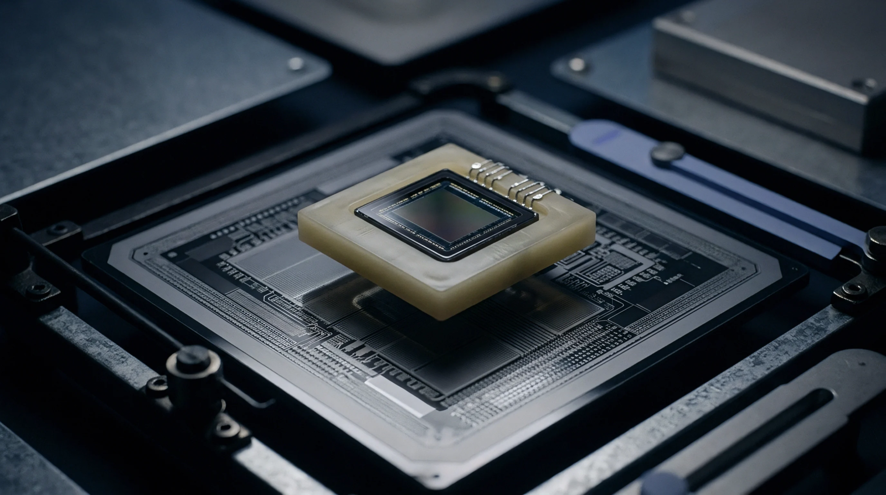
Assembly Stage
Semiconductor manufacturing involves the physical bonding of a processed silicon disc to a carrier or a substrate. The wafer attach process ensures a rigid and thermally conductive connection that survives subsequent dicing and packaging steps. High-precision adhesives or metallic alloys are used to create this interface.
Bonding Chemistry
Chemical properties selected for the interface must match the thermal expansion coefficients of the silicon and the carrier. During wafer attach, the application of heat and pressure activates the bonding agent to form a permanent seal. The thickness of the bond line is controlled to within a few micrometers to maintain the planar alignment of the assembly.
Quality Control
Voids or delamination within the bond layer can lead to catastrophic failure during operation. Inspection of the wafer attach is performed using scanning acoustic microscopy to detect any air pockets or cracks. Shear strength testing provides a quantitative measure of the bond integrity against the specified requirements.
Thermal resistance measurements also verify that the interface can effectively pull heat away from the active circuits. If the thermal gradient is too high, the process parameters are adjusted to improve the coverage of the adhesive.
Alignment Precision
In high-density applications, the wafer attach requires sub-micron accuracy to ensure that the through-silicon vias line up with the substrate pads. Automated pick and place machines use fiducial markers to achieve this level of repeatability.