Interconnect Format
An integrated circuit package utilizes a grid of flat metal pads on its underside instead of pins or solder balls. This lga package offers a lower mounted height and better electrical performance than leaded alternatives. The low inductance of the flat contacts makes it ideal for high frequency and high speed applications.
Solder paste is applied directly to the printed circuit board pads before the device is placed.
Thermal Path
The lack of leads allows for a direct thermal path from the package body to the circuit board copper planes. This design enables efficient heat dissipation from high power processors and modules. Designers often include a matrix of thermal vias beneath the package to conduct heat to the bottom board layer.
Assembly Process
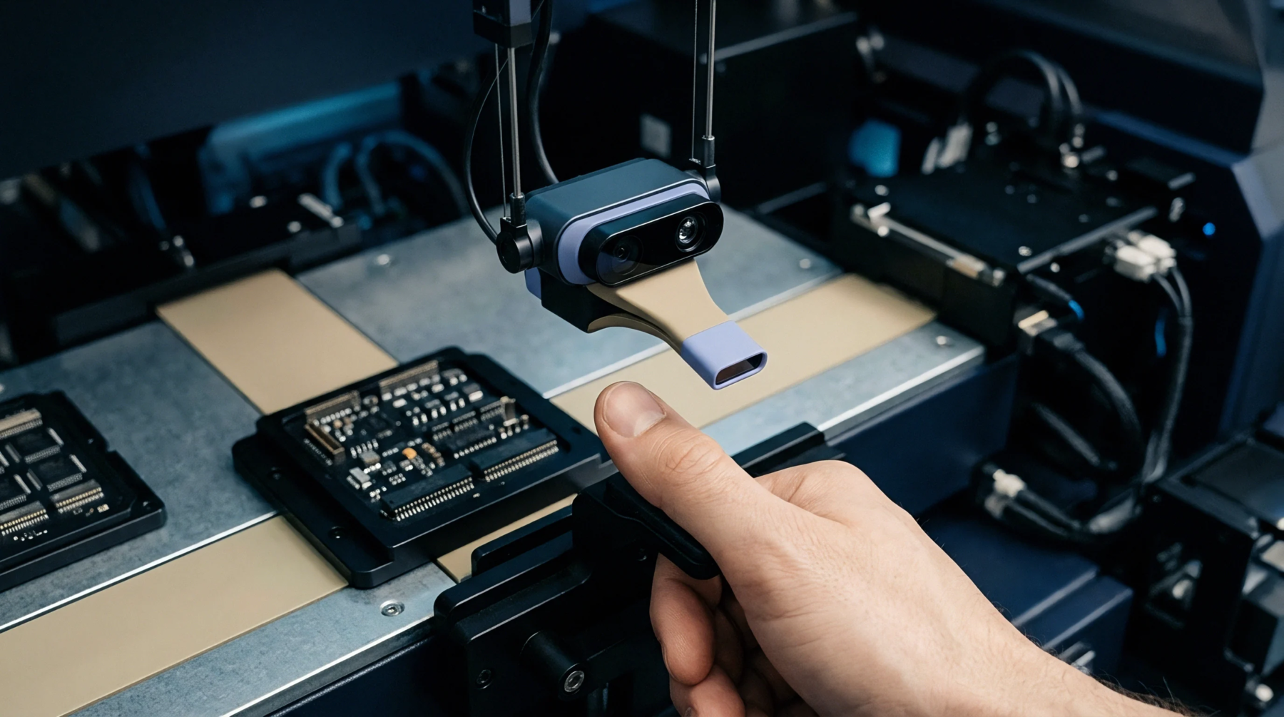
Surface mount assembly requires precise solder paste deposition to prevent open connections or bridging between the closely spaced pads. Automatic pick and place machines position the device with high accuracy to align with the board pads. Reflow profiles must be carefully managed to ensure uniform heating across the entire grid.
Automated optical systems inspect the perimeter joints, while x-ray systems are used to verify the hidden inner joints.
Solder Joint Stress
The rigid connection between the package and the board makes the assembly vulnerable to thermal expansion mismatches. Under thermal cycling, the solder joints can experience significant fatigue and crack. Selecting board materials with compatible thermal expansion coefficients reduces this risk.