Footprint Standard
Printed circuit board design standards define mathematical models for surface mount land pattern geometries. IPC-7351 provides standardized pad dimensions based on component tolerances and assembly density levels. Adherence to these guidelines ensures consistent solder fillet formation during automated assembly.
Solder Joint
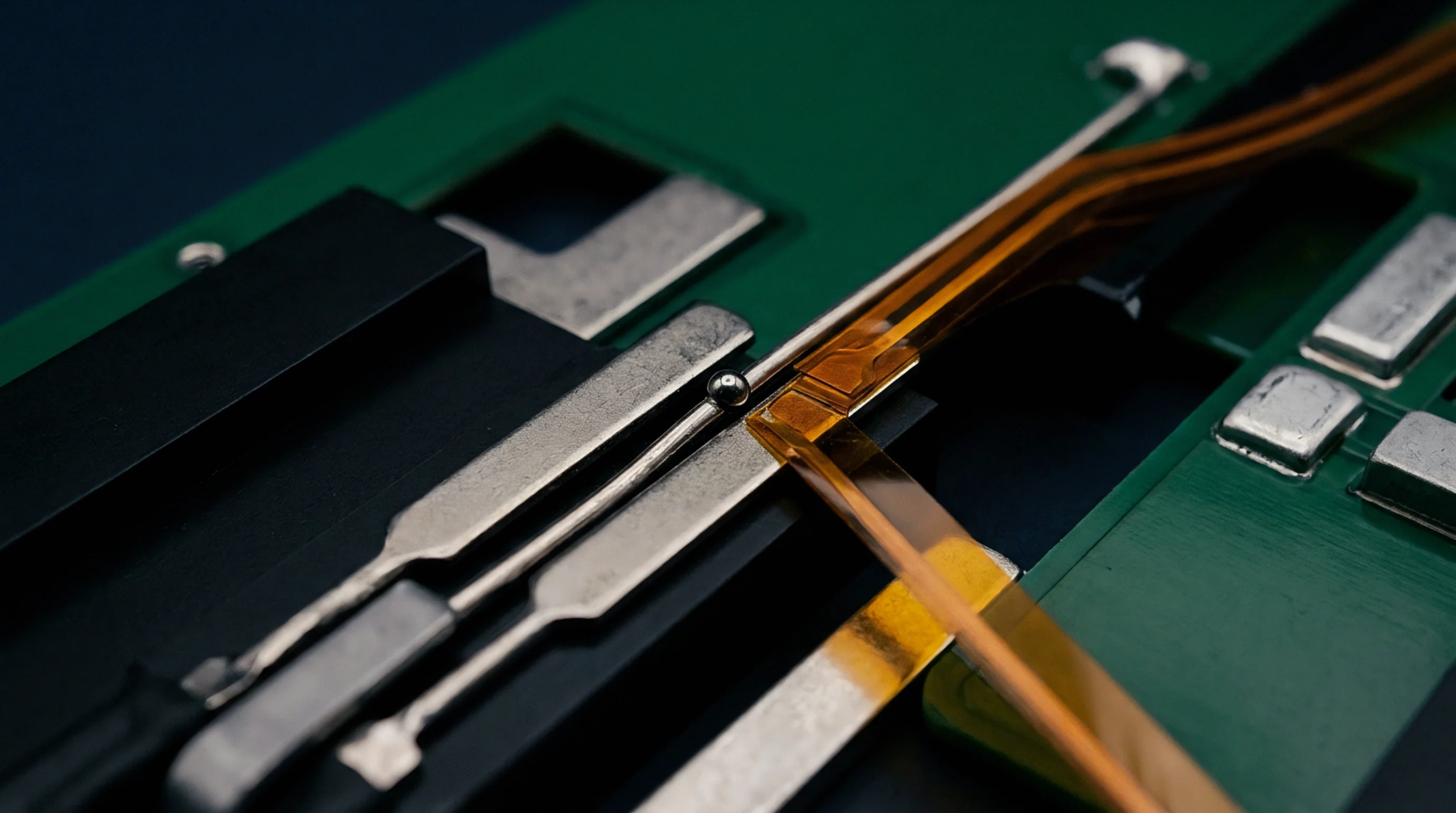
Land patterns dictate solder volume distribution between component terminations and circuit board copper pads. Incorrect pad sizes lead to manufacturing defects such as component tombstoning, solder bridging or insufficient fillet height. The specification establishes three density levels (most, nominal, least material conditions) to accommodate varying manufacturing process capabilities and product reliability requirements.
Tolerance Envelope
Calculations incorporate component manufacturing tolerances, board fabrication tolerances and placement equipment accuracy. Component body dimensions and lead tolerances determine the minimum required land pattern size. Standardized formulas compute toe, heel and side solder joint goals for every surface mount package class.
Placement Yield
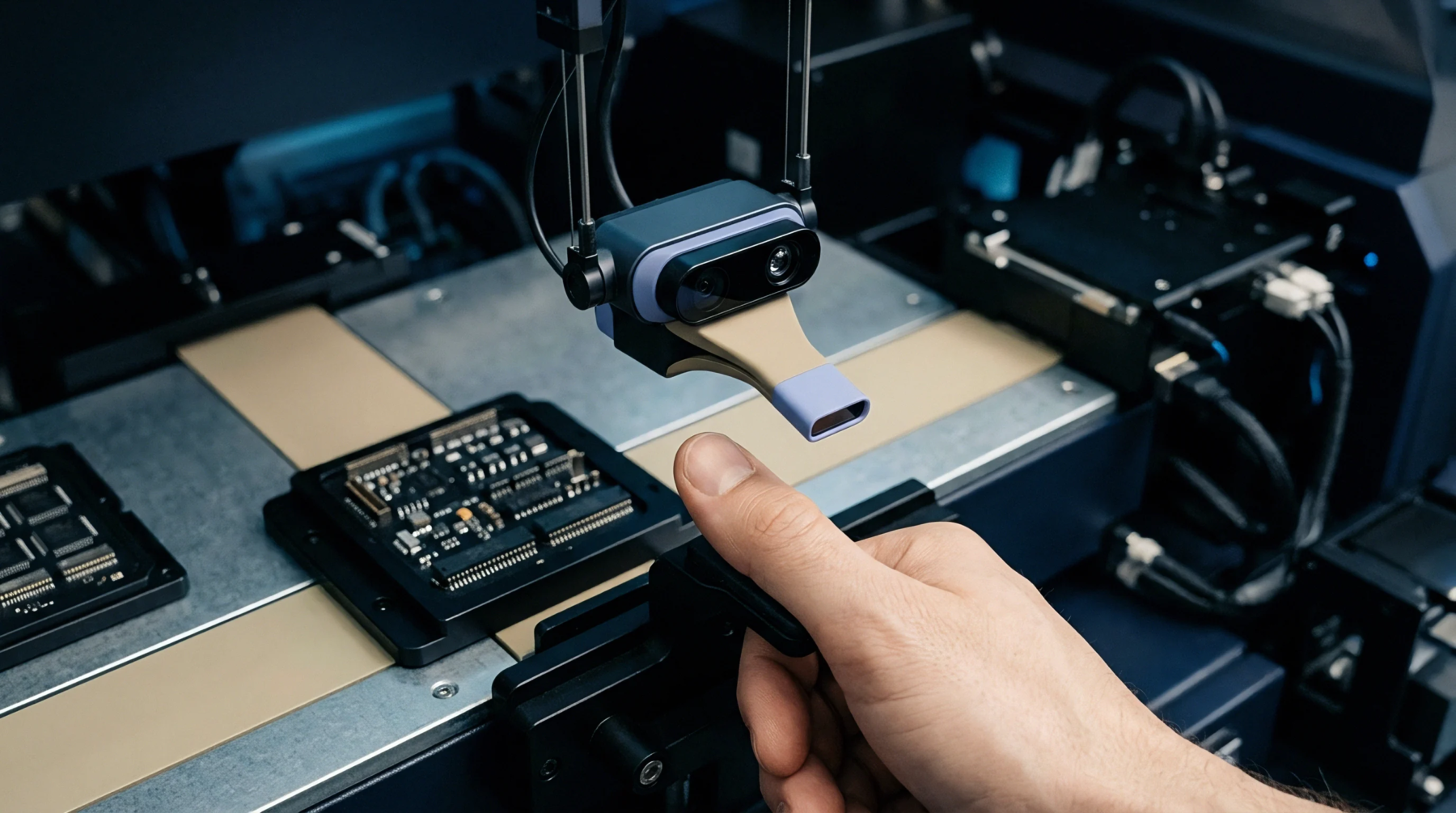
Automated pick-and-place equipment relies on standardized land pattern libraries to achieve high placement yield without manual board corrections. Consistent pad geometry reduces mechanical stress on solder joints during thermal cycling and vibration exposure. CAD library generators implement these standardized equations to automate footprint creation for complex micro-BGA and QFN packages.
Qualification procedures check solder joint geometry against visual acceptance criteria. IPC-7351 guidelines streamline automated printed circuit board assembly processes.