Package Footprint
Surface mount microelectronic packaging utilizes a twelve-contact land grid array configuration to minimize the footprint of miniature sensing devices. This design has no pins, relying instead on flat metal pads on the bottom of the package. Sourcing the LGA-12 package enables compact system design in space-constrained industrial and consumer applications.
Pin Allocation
Specific pad assignments are designated for power supply, ground, clock and digital communication interfaces. The symmetric placement of these contacts requires a clear orientation mark on the package to ensure correct board alignment.
Contact Resistance
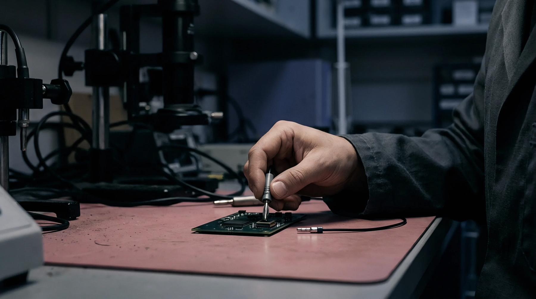
Uniform pressure and precise solder volume are critical to establishing low resistance electrical connections across all twelve pads. Non-uniform solder paste deposition can lead to open circuits or intermittent contact failures under thermal cycling. Technicians utilize multi-point resistance measurements to evaluate the quality of the soldered joints during qualification runs.
The mechanical stability of the joint is influenced by the composition of the solder alloy and the surface finish of the lands.
Mechanical Retention
The absence of solder balls means the package sits closer to the circuit board, reducing parasitic inductance. This low profile improves signal integrity but increases the susceptibility of the solder joint to shearing forces.