Housing Design
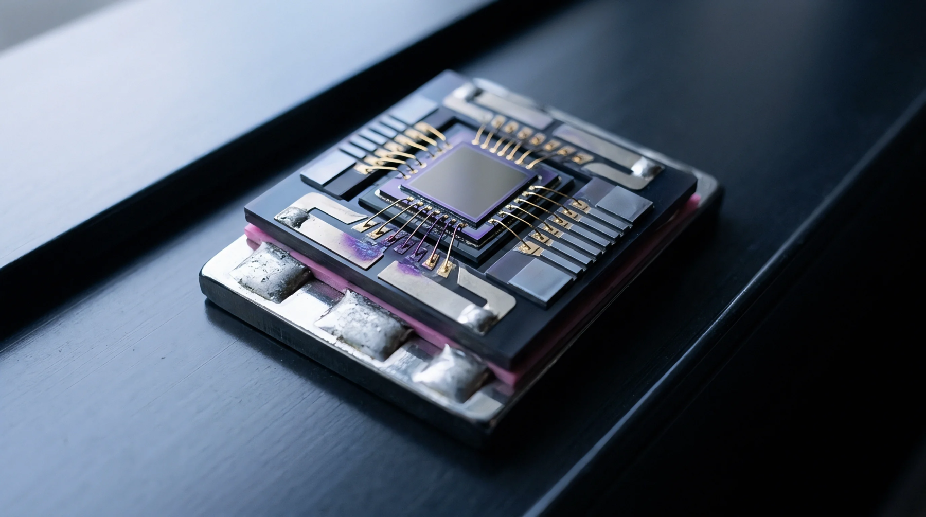
Plastic encapsulated packages employ leadless terminals on all four sides of the component base to improve thermal dissipation and high frequency performance. The qfn or quad flat no lead package consists of a silicon die mounted on a leadframe and covered with a molding compound. Unlike traditional packages with protruding pins, the electrical contacts are located on the underside, flush with the edge of the plastic body.
This design results in a very small footprint and a low profile, making it ideal for compact mobile devices and high speed digital circuits. The lack of external leads reduces the parasitic inductance and capacitance of the package, which allows the device to operate at higher frequencies with less signal degradation. This format has become a standard for everything from microcontrollers to radio frequency power amplifiers.
Terminal Layout
Arrangement of the contact pads around the perimeter of the base provides a high number of connections in a very small area. Most quad flat no lead packages also feature a large exposed pad in the center of the underside. This central pad serves as a primary thermal path, allowing heat to flow directly from the silicon die into the printed circuit board.
It is also often used as a ground connection to improve the electrical stability of the device. The solder joints for the perimeter pads are partially visible on the side of the package, which helps with visual inspection after the reflow process. However, the quality of the joint under the component remains difficult to verify without the use of x ray equipment.
The fine pitch of the pads requires high precision during the stencil printing and the component placement steps.
Soldering Performance
Attachment of the package to the substrate relies on a carefully controlled reflow cycle to ensure that all pads are properly wetted with solder. One common issue with this package style is the tendency for the component to float or tilt if the amount of solder paste on the central pad is not correctly balanced. This can lead to open circuits on the signal pins or poor thermal contact with the heat sink.
To prevent this, designers often use a grid of small solder mask openings instead of one large one for the central pad. This helps to manage the surface tension of the molten solder and keeps the component level. The low standoff height also makes it difficult to clean away any flux residue that might be trapped under the body, necessitating the use of no clean solder pastes.
Parasitic Reduction
Superior electrical characteristics of the leadless design make it the preferred choice for high speed and high frequency applications. By eliminating the long wire bonds and lead frames found in older packages, the qfn minimizes the delays and reflections that can plague fast digital signals. The large ground pad also provides a very low impedance path for return currents, which reduces electromagnetic interference and improves the signal integrity.
This combination of thermal efficiency and electrical performance is why the package is so widely used in modern power management and communication systems. It represents a mature and reliable technology that continues to meet the needs of the most demanding electronic designs. The package is a staple of contemporary hardware architecture, offering a versatile and cost effective housing for a vast range of integrated circuits.