
Digital Interface Signal Integrity and Bus Capacitance Optimization
Optimizing bus capacitance demands matching package pin loading and trace geometry against pull-up resistance limits to guarantee rise time margins.
Optimizing bus capacitance demands matching package pin loading and trace geometry against pull-up resistance limits to guarantee rise time margins.
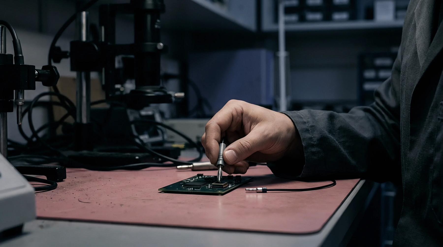
Land pattern calibration adjusts pad geometry for stencil limits and reflow strain to maintain sensor zero-point stability.

Bottom terminated package parasitic isolation requires thermal pad segmentation while mechanical stress drift is suppressed by limiting solder voiding under 10 percent.

Interconnect parasitic shifts degrade return loss and collapse eye margins, forcing board-level copper compensation and firmware-driven equalization offsets.
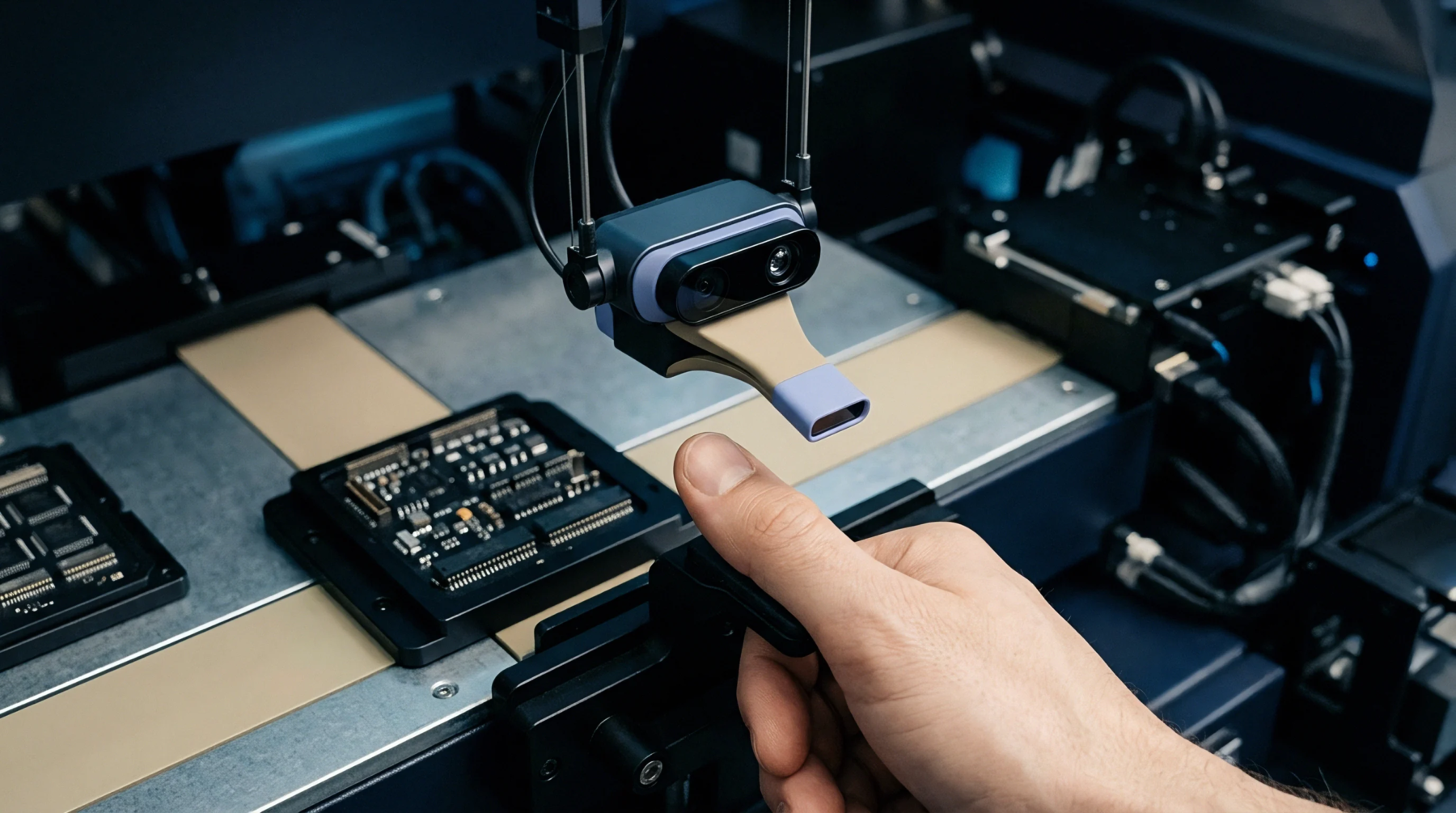
Extract leadless package parasitics using 3D field solvers and route unbroken ground returns under thermal pads to suppress inductive ground bounce.

Dynamic strain rate matrix models show low-temperature Bi-Sn solders embrittle at impact velocities, requiring micro-alloying or underfill to pass drop audits.

Triaxial strain rosette signal acquisition during depaneling audits requires simultaneous 50 kHz sampling and 10 kHz anti-aliasing filtering to capture true strain peaks.
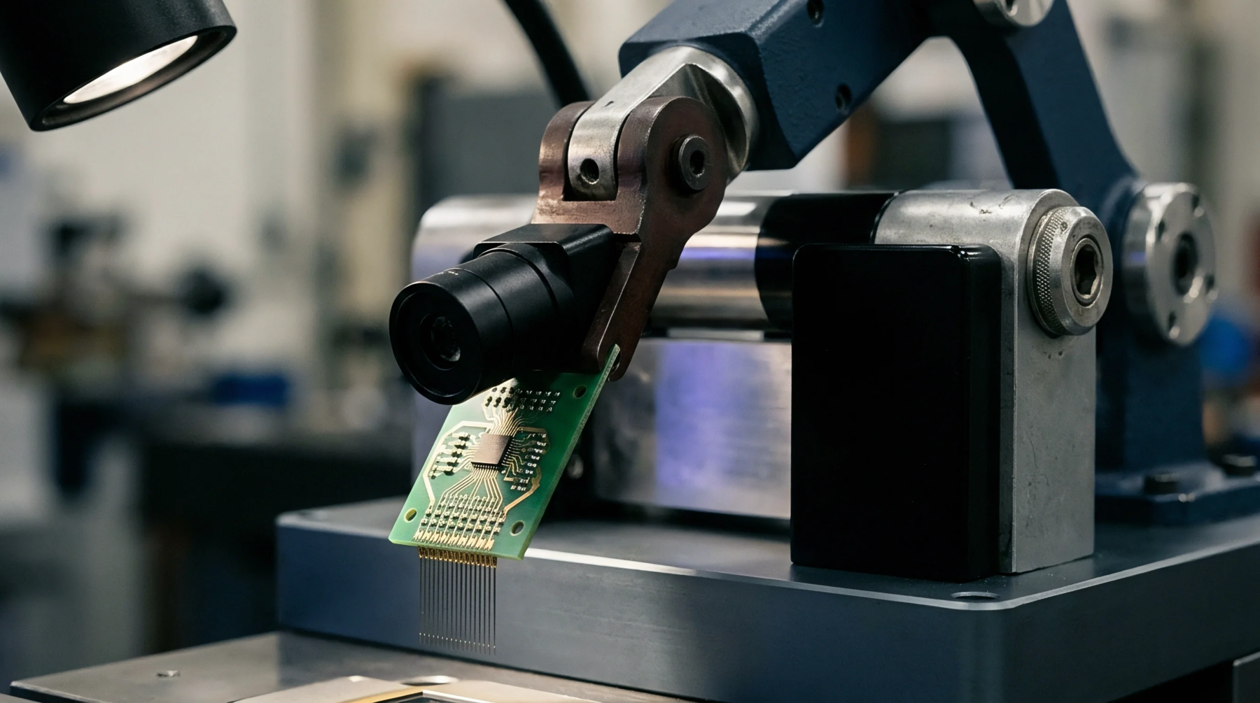
Surface mount strain gauge selection relies on matching package shear modulus, serial bus update rates, and IPC-9704 board strain limits.

Characterizing substrate interface viscoelastic shear relaxation prevents dynamic thermal offset drift and avoids expensive late stage packaging redraws.

Finite element modeling of underfill creep uses Prony viscoelasticity and Anand viscoplasticity to predict and compensate long-term silicon sensor drift.

Polymer viscoelastic stress relaxation in molded MEMS packages causes long-term zero-point offset drift that requires cavity isolation or baked burn-in.

Unbalanced copper planes and high-modulus die attach adhesives in laminate sensor packages cause reflow-induced warpage that shifts piezoresistive zero points.

Discrete transducer SMT yield loss and calibration costs depend on pad symmetry, post-reflow strain aging, and test cell chamber dwell times.

Discrete sensor chip-down integration breaks even above fifteen thousand units where bill-of-materials savings overcome tooling and test fixture outlays.

Automated boundary scan extraction combined with transmissive X-ray die metrology catches silent silicon stepping changes before SMT placement lines fault.

Trap hardware stepping errata by verifying silicon ID registers during boot and driving high-side rail switches to clear frozen bus states.

Silicon revisions alter open-drain driver impedance and state timing, turning compliant clock stretching into bus-halting race conditions across fast edges.

Elastomer creep alters baseline compressive stress on MEMS packages, causing long term zero drift that requires digital firmware offset compensation.
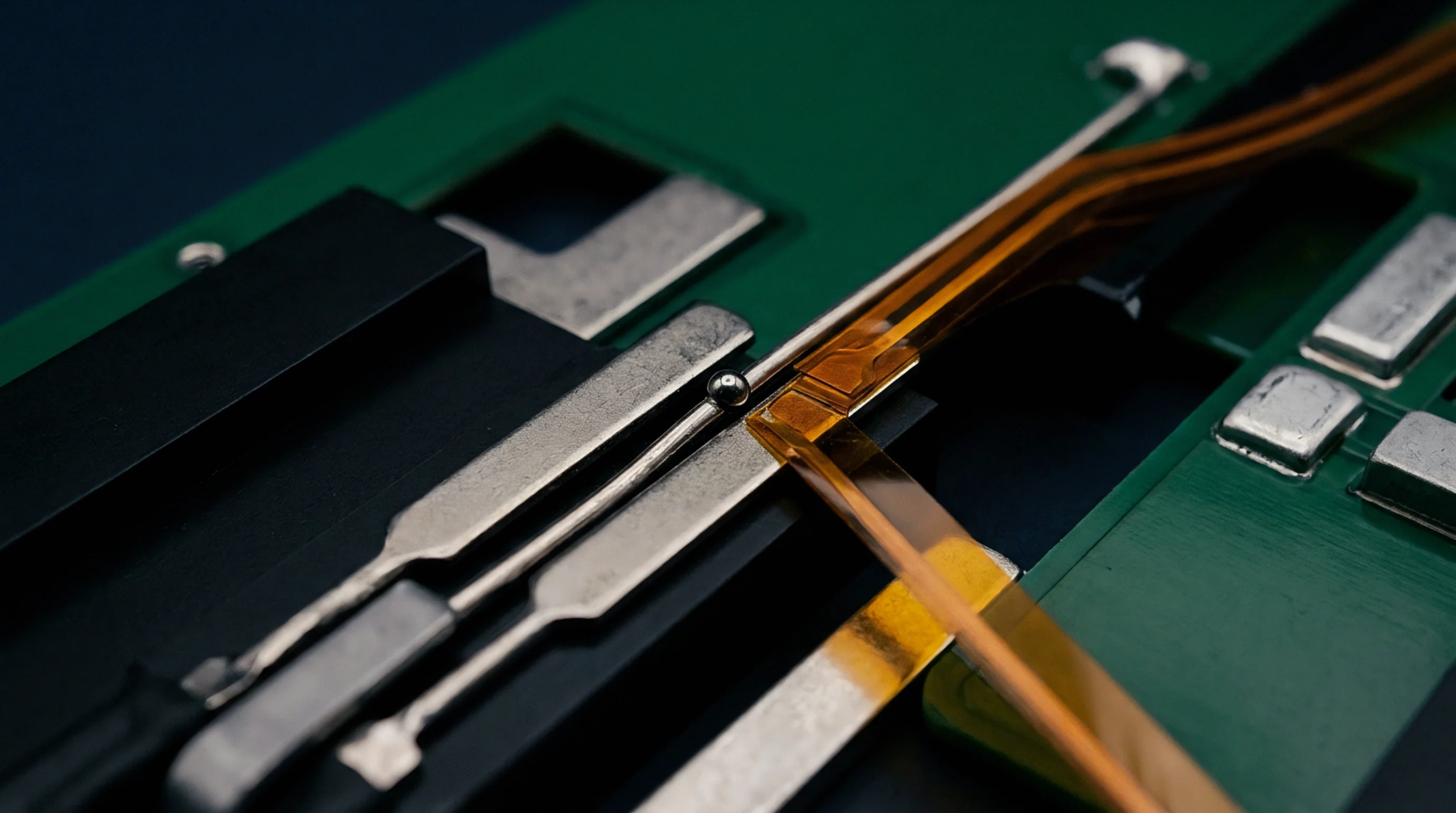
Milled PCB isolation slots and controlled solder standoff heights decouple surface mount pressure sensors from assembly flexure and thermal board strain.

Optimizing transducer port sealing demands balancing 15 to 25 percent gasket squeeze against volumetric fill below 85 percent to prevent mechanical die offset.

Polymeric underfill modulus collapse near glass transition increases board strain attenuation while driving out-of-plane bump fatigue and sensor drift.

Analytical shear lag models quantify strain transfer from boards to bottom-terminated packages, showing compliant die attach drops offset drift by 98 percent.

Surface strain fields across deflecting circuit boards scale with distance from the neutral axis and concentrate sharply at stiff component perimeters.

WLCSP packaging induces mechanical stress gradients that shift bandgap references, requiring rotated common-centroid layouts and active digital trim.

Mitigate bandgap thermal stress errors using compliant leaded packages, PCB isolation slots, polyimide die buffers, and stabilized factory calibration.

Cross-quad common-centroid bandgap layouts cancel linear thermal gradients, while PCB isolation slots prevent package piezoresistive strain from shifting Vbe drift.

Mitigate surface-mount precision reference thermomechanical drift using three-sided PCB slot moats, compliant land patterns, or hermetic ceramic packages.

Optimized PCB slotting isolates precision voltage references from board strain and thermal gradients, cutting drift below one part per million.
Precision voltage reference accuracy depends on isolating packages from board flexure, balancing trace Seebeck junctions, and blocking thermal conduction paths.

Quantifying timing budget degradation across multi-channel I2C switches requires auditing accumulated branch capacitance against pull-up rise time limits.
Expertise is a utility, not a secret. sentiention™ publishes its working knowledge as open reference: intelligence layer covering the materials it sources, the markets it enters, and the reference that serves both.